- STMicroelectronics Community
- STM32 MCUs
- STM32 MCUs Products
- Re: All 0x00 in STM32G4 flash? Is it can be recove...
- Subscribe to RSS Feed
- Mark Topic as New
- Mark Topic as Read
- Float this Topic for Current User
- Bookmark
- Subscribe
- Mute
- Printer Friendly Page
All 0x00 in STM32G4 flash? Is it can be recover?
- Mark as New
- Bookmark
- Subscribe
- Mute
- Subscribe to RSS Feed
- Permalink
- Email to a Friend
- Report Inappropriate Content
2021-01-11 4:34 AM
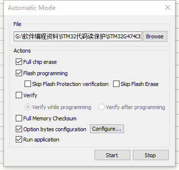
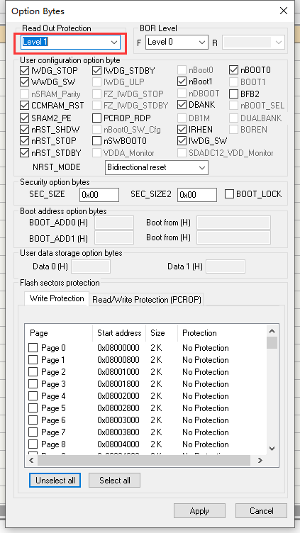
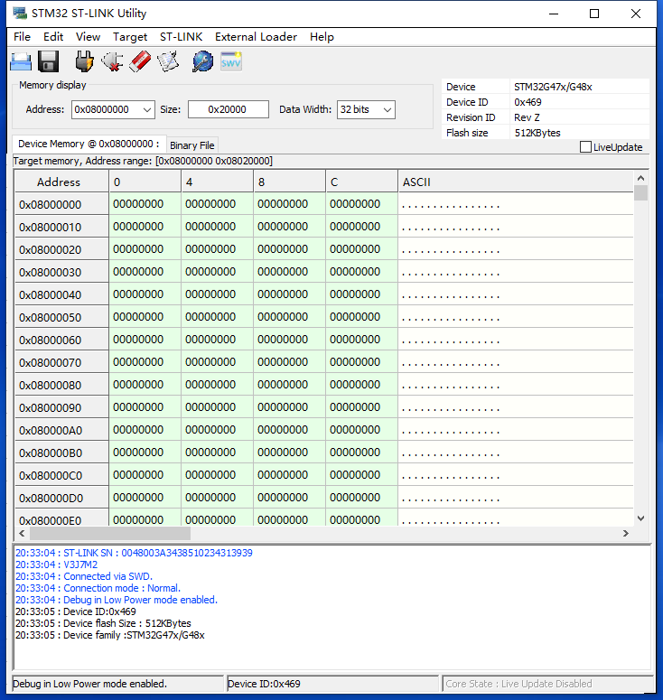
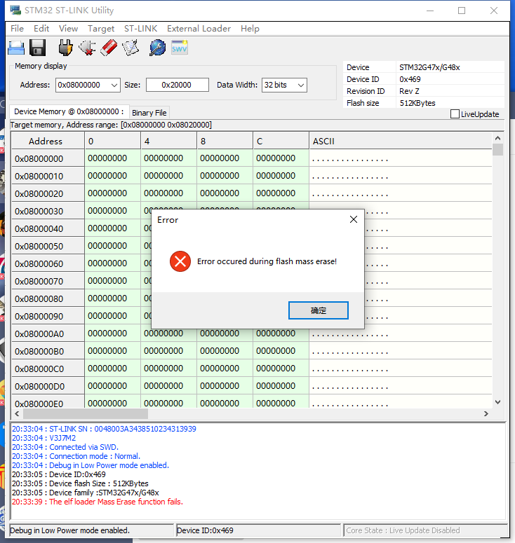
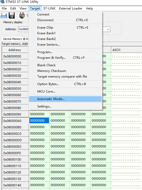
I am testing STLINK Utility's Automatic Mode for mass-production,I set read out protection in option byte from level0 to level1(I have never set it to level2,for its irreversibility),so I just plug in and out the STLINK acting as the operation of mass-production.The times are less than 30(in my memory),but at last I find the flash contents are all 0x00 in flash(starting from 0x08000000,with the legth of the max size of 512K flash).I tried to revise the read out protection to level0(without read out protection),I could see the contents are all 0x00 all the same no matter what I tried,such as full chip erease , page erease or programing new hex file,the flash could not be revise,they are all 0x00.
So anyone can help me? My ST chip is STM32G474E DPOW discovery on board chip,thanks.
Solved! Go to Solution.
- Labels:
-
STM32G4 series
Accepted Solutions
- Mark as New
- Bookmark
- Subscribe
- Mute
- Subscribe to RSS Feed
- Permalink
- Email to a Friend
- Report Inappropriate Content
2021-01-14 6:58 PM
Now I will share the method how I reset the STM32G4's FLASH BANK RDP:
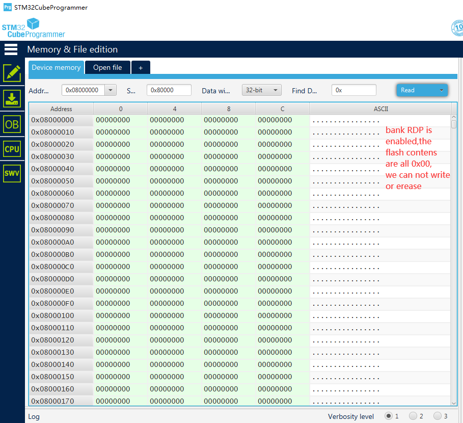
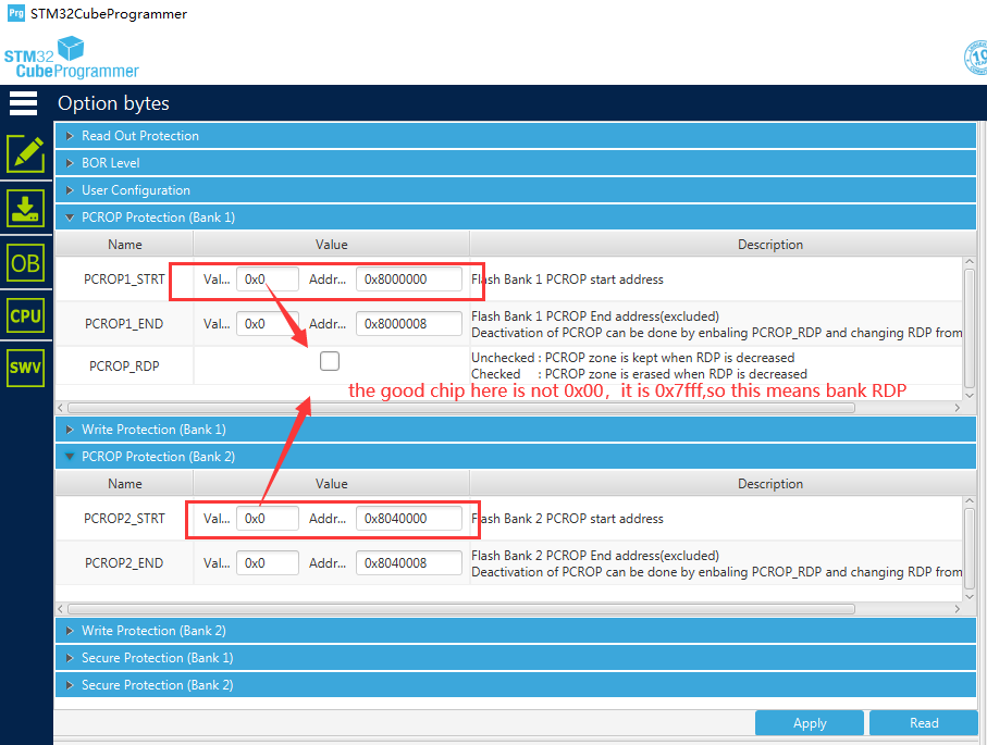
the firgure below is the BANK RDP falsh statue, it could not be written or ereased,and the contents are all 0x00 when read;
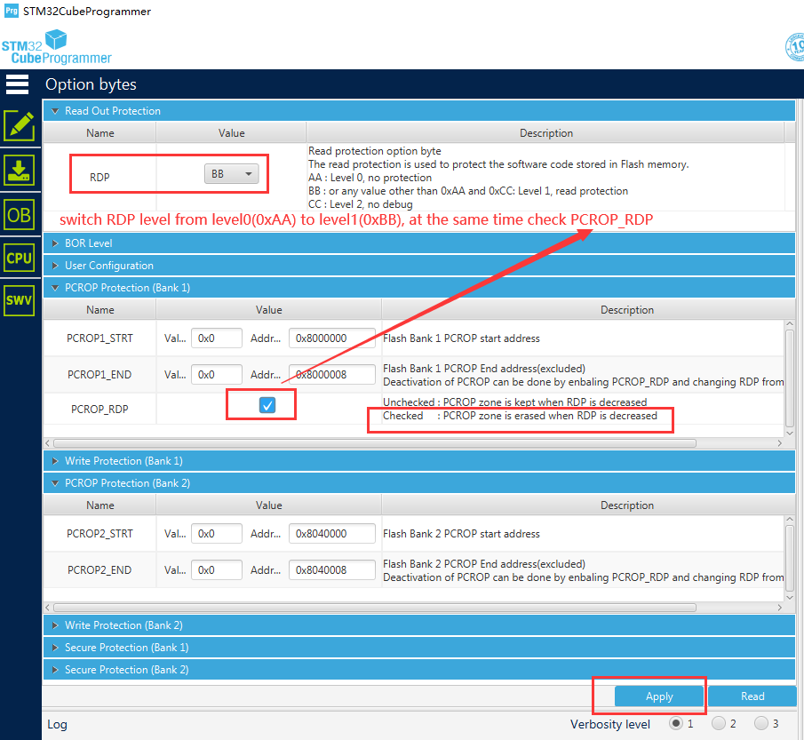
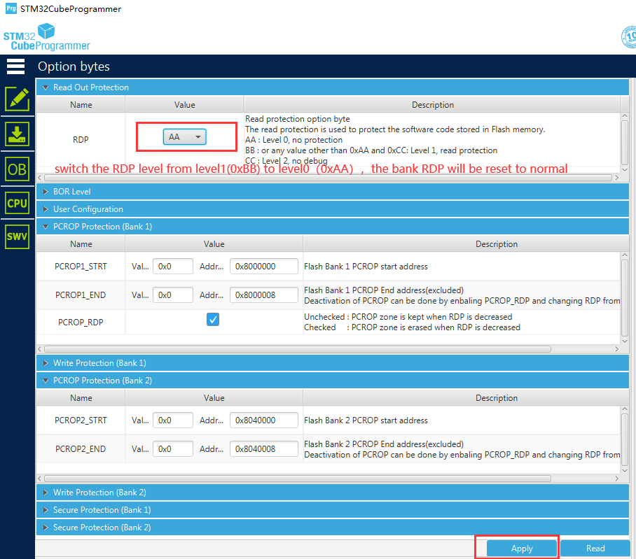
1.check the PCROP_RDP , at the same time set the RDP level from level0(0xAA) to level1(0xBB),according to the PCROP_RDP(Checked :PCROP zone is erased when RDP is decreased), then apply the option byte revisition to make it effective.
2.then set the RDP level from level1(0xBB) to level0(0xAA),apply the option byte revisition to make it effective.
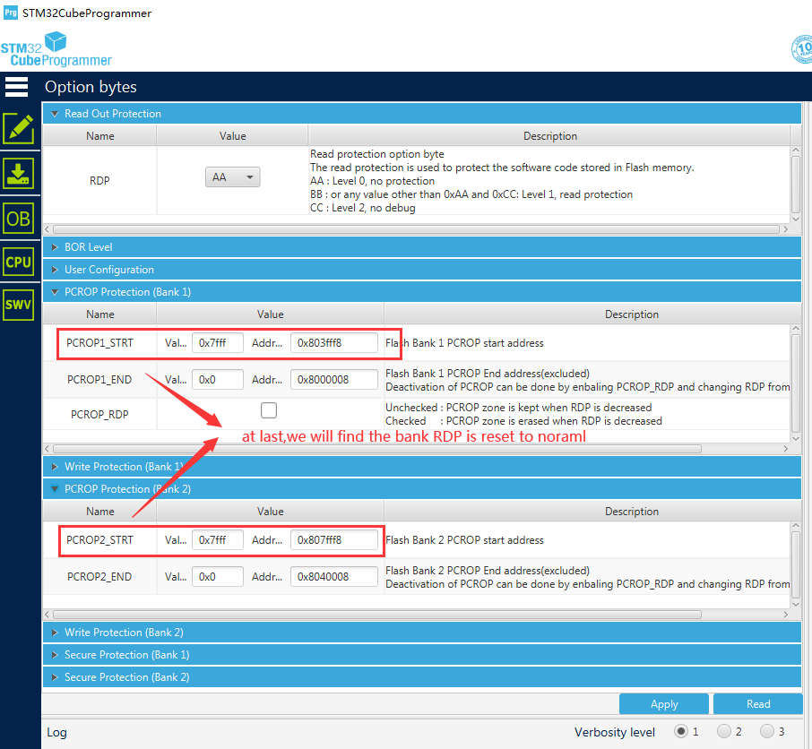
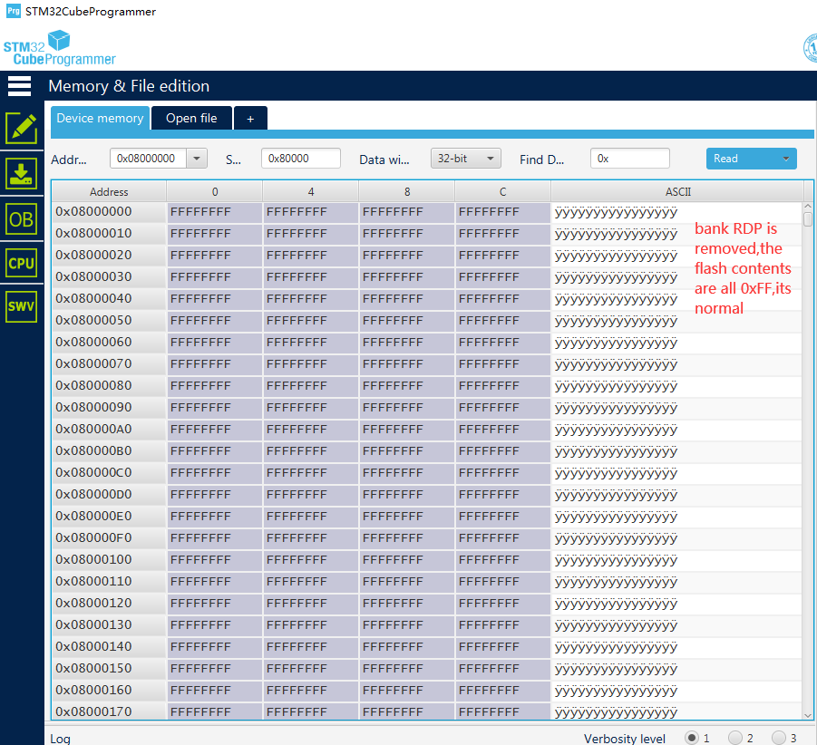
at last, we will find the BANK RDP configuration is reset to noraml, the falsh contents are all 0xFF,witch could be written and ereased again.
- Mark as New
- Bookmark
- Subscribe
- Mute
- Subscribe to RSS Feed
- Permalink
- Email to a Friend
- Report Inappropriate Content
2021-01-12 6:42 PM
I have asked the ST‘s enginerer,the 3v3 power supply of MCU shoulud be Ensured stable during flash ereasing and writing.I decide to replace the chip.
- Mark as New
- Bookmark
- Subscribe
- Mute
- Subscribe to RSS Feed
- Permalink
- Email to a Friend
- Report Inappropriate Content
2021-01-13 7:57 PM
With the mentality of having a try, I compare the option byte of this chip with that of a good chip,I finally find the problem is bank RDP,causing by unstable power supply when program flash and option byte.I will share the method of recovery of the option byte to normal state.
- Mark as New
- Bookmark
- Subscribe
- Mute
- Subscribe to RSS Feed
- Permalink
- Email to a Friend
- Report Inappropriate Content
2021-01-14 6:58 PM
Now I will share the method how I reset the STM32G4's FLASH BANK RDP:
the firgure below is the BANK RDP falsh statue, it could not be written or ereased,and the contents are all 0x00 when read;


1.check the PCROP_RDP , at the same time set the RDP level from level0(0xAA) to level1(0xBB),according to the PCROP_RDP(Checked :PCROP zone is erased when RDP is decreased), then apply the option byte revisition to make it effective.

2.then set the RDP level from level1(0xBB) to level0(0xAA),apply the option byte revisition to make it effective.

at last, we will find the BANK RDP configuration is reset to noraml, the falsh contents are all 0xFF,witch could be written and ereased again.


- Unable to Connect to NUCLEO-STM32H7S3L8 in STM32CubeProgrammer or STM32CubeIDE in STM32 MCUs Products
- Flashing Issue with STM32G431RB in IAR Embedded Workbench 8.22.3 After Patch Installation in STM32 MCUs Products
- Issue with Flashloader after applying the IAR patch to Support STM32G4 in IAR 8.22 in STM32CubeProgrammer (MCUs)
- Trying to understand the cycle count on my STM32G431 code in STM32 MCUs Products
- UART bootloader no magic byte after mass erase in STM32 MCUs Embedded software
