Address mapping of 1GBit of continuous memory (Parallel NOR Flash M29EW) - FSMC/FMC
- Mark as New
- Bookmark
- Subscribe
- Mute
- Subscribe to RSS Feed
- Permalink
- Email to a Friend
- Report Inappropriate Content
2018-09-12 9:41 AM
Hello Folks!
So far, I've been able to utilize the FSMC/FMC peripheral in many different scenarios, including interfacing LCDs in 8080 mode, legacy ASICs, SDRAMs, etc. I'm now working on a project that involves M29EW Parallel NOR Flash (1GB single-die TSOP) and I was wondering if the FMC (STMF429) can address 1 GB of continuous memory space. As far as I know, BANK 1 of the FMC that is dedicated for the NOR-type of memory is divided across 4 sub banks with an individual chip-select (NE) for each bank. With that being said, if I have configured the FMC for 26 address bits on a given NE, would it be possible then to address a 1-GBit (128 MBytes) of continuous memory space?
Thanks,
Zaher
- Mark as New
- Bookmark
- Subscribe
- Mute
- Subscribe to RSS Feed
- Permalink
- Email to a Friend
- Report Inappropriate Content
2018-09-12 9:55 AM
For the 0x60000000..0x6FFFFFFF space is broken into 4x 64MB blocks, you'd have to reconstruct high order address bits, and AND a pair of NEx together
Up vote any posts that you find helpful, it shows what's working..
- Mark as New
- Bookmark
- Subscribe
- Mute
- Subscribe to RSS Feed
- Permalink
- Email to a Friend
- Report Inappropriate Content
2018-09-12 11:38 AM
Great idea. This way we could combine two sub-banks for a total of 128MB address space. But could you please elaborate more on this by a simple schematic or block diagram? Why AND and not OR? When application calls for write on address space higher than the first 64MB (sub-bank 2) how many address bits are enabled/set by then?
Quote: "you'd have to reconstruct high order address bits" Please try to provide more details.
Thanks
- Mark as New
- Bookmark
- Subscribe
- Mute
- Subscribe to RSS Feed
- Permalink
- Email to a Friend
- Report Inappropriate Content
2018-09-12 11:49 AM
By the way, it seems CubeMx has no problem configuring the FMC for a NOR flash with 26-bits of address lines on a single NEx.
- Mark as New
- Bookmark
- Subscribe
- Mute
- Subscribe to RSS Feed
- Permalink
- Email to a Friend
- Report Inappropriate Content
2018-09-12 12:46 PM
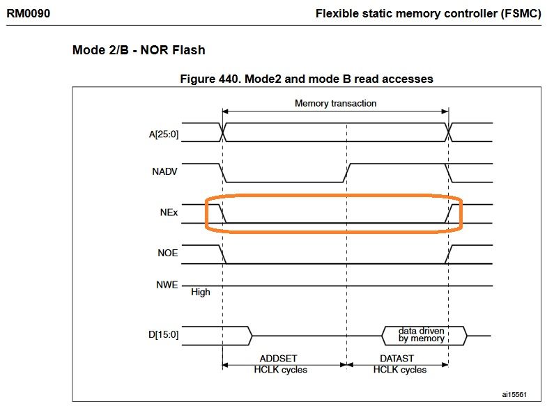
I think FSMC_NEx are negative going, you want the -CE zero if either of the -NE1 or -NE2, an OR's not going to get that job done.
>>Quote: "you'd have to reconstruct high order address bits" Please try to provide more details.
A25 = FSMC_NE1, cause it will be LOW for the bottom half of the address space, and HIGH for the top half.
Up vote any posts that you find helpful, it shows what's working..
- Mark as New
- Bookmark
- Subscribe
- Mute
- Subscribe to RSS Feed
- Permalink
- Email to a Friend
- Report Inappropriate Content
2018-09-12 12:51 PM
All the address bits might be exposed, and shifted for 16-bit wide data bus, I'm just not willing to guarantee that.
Up vote any posts that you find helpful, it shows what's working..
- Mark as New
- Bookmark
- Subscribe
- Mute
- Subscribe to RSS Feed
- Permalink
- Email to a Friend
- Report Inappropriate Content
2018-09-12 4:41 PM
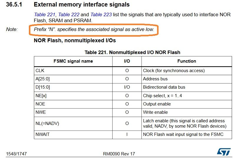
Do you mean the NEx signals are active low? Thanks for the tip, but I would like to see a reference to that in the datasheet or reference manual of the device.
So, there's a big chance to work out of the box, without extra logic? I believe it's worth a try. At least, if it didn't work, I guess I won't have problem accessing the first 64MB space of the M29EW flash chip.
- Mark as New
- Bookmark
- Subscribe
- Mute
- Subscribe to RSS Feed
- Permalink
- Email to a Friend
- Report Inappropriate Content
2018-09-12 8:08 PM
>>Thanks for the tip, but I would like to see a reference to that in the datasheet or reference manual of the device.
You might want to look at the RM then.
Up vote any posts that you find helpful, it shows what's working..
- Mark as New
- Bookmark
- Subscribe
- Mute
- Subscribe to RSS Feed
- Permalink
- Email to a Friend
- Report Inappropriate Content
2018-09-13 11:03 AM
Mr. Clive, you are our best reference of information over here. I just wanted you to show me where it was covered in the RM as I couldn't find it.
Anyways, I hope you bear with me a little bit and explain it with a bit more of details. From the M29EW datasheet, it seems the A[26:0] address inputs are ACTIVE HIGH. When write takes place on the top half (second 64MB sub-bank), FMC_NE1 goes high and this applies to A25 of the M29EW? Now, CE# is ACTIVE LOW for the M29EW. I can see now why AND is required on a pair of NEx signals, but I'm still confused regarding the "reconstructing" of the address bits as you suggested, and which goes to which?
Just wanted to make sure everything is correct before I start designing the PCB.
Thank you again for your excellent follow up!
- Mark as New
- Bookmark
- Subscribe
- Mute
- Subscribe to RSS Feed
- Permalink
- Email to a Friend
- Report Inappropriate Content
2018-09-13 11:55 AM
Review the state of the pins during the bus transaction. Apply "logic". Remember FSMC_NE1 and FSMC_NE2 will ONLY be LOW during active accesses to the NOR, the entirety of the rest of time they will be HIGH. Only ONE will be LOW at a time.
You don't provide a datasheet or part# for the specific part you're using, but I'm assuming an 16-bit wide device (D0..D15) with address (A0..A25) describing 128MB in total. And in this case you'd connect A25 with FSMC_NE1, because FSMC_NE1 will be ZERO during access to the lower 64M bank, and HIGH when FSMC_NE2 is LOW for the second 64M bank.
Up vote any posts that you find helpful, it shows what's working..

