- STMicroelectronics Community
- STM32 MCUs
- STM32 MCUs Embedded software
- Interfacing external FIFO with STM32F767ZI to shif...
- Subscribe to RSS Feed
- Mark Topic as New
- Mark Topic as Read
- Float this Topic for Current User
- Bookmark
- Subscribe
- Mute
- Printer Friendly Page
Interfacing external FIFO with STM32F767ZI to shift ip camera data into FPGA
- Mark as New
- Bookmark
- Subscribe
- Mute
- Subscribe to RSS Feed
- Permalink
- Email to a Friend
- Report Inappropriate Content
2018-10-10 12:57 AM
Dear all,
I have an IP Camera which i have interfaced with STM32F767ZI. I m able to command the camera over ethernet (RTSP) and recieve RTP packets containing video data over UDP. Further i wish to interface STM32F767ZI with 2 FIFOs . These FIFOs will be used to store video data (ie. payload of RTP packets). The FIFOs will be read by FPGA and further processing on data will be done on FPGA.(Two FIFOs are required so that while 1 FIFO is being written by MCU , the other is to read by FPGA . Hence there will be no loss of packets).
My probelm is I wish to write FIFO at high frequency so that no UDP ethernet packets are lost. For this i want 32 bit data to be pushed to FIFO with highest possible frequency clock. Can you please help me write a code in C to synchronously shift 32bit data into my external FIFO.
Solved! Go to Solution.
- Labels:
-
Ethernet
-
STM32F7 series
Accepted Solutions
- Mark as New
- Bookmark
- Subscribe
- Mute
- Subscribe to RSS Feed
- Permalink
- Email to a Friend
- Report Inappropriate Content
2018-10-24 3:42 AM
the best way forward is to reduce the complexity.
this is untested, syntax errors abound.... just off the top of my ears
referencing your stuff:
#define WRITE_READ_ADDR     ((uint32_t)0x0800)
#define BUFFER_SIZE         ((uint32_t)0x01F4)
#define SRAM_BANK_ADDR ((uint32_t)0X60000000)

char* destPtr = SRAM_BANK_ADDR | WRITE_READ_ADDR ;

while (1){

	*destPrt = 0x50;  // write data
	*destPrt = 0x52;  // write data
	*destPrt = 0x56;  // write data
	*destPrt = 0x57;  // write data
	*destPrt = 0x5F;  // write data

	HalDelay(1);	// not sure on the syntax, I dont use delays... :(
}
This should give you a stable Scope image of 5 transactions. repeating every mS
now you should see transfers at about 40-60MHz,
that is @50MHz is 20nS per cycle, 5 cycles, is about 100nS of data, then pause for 1mS.
- Mark as New
- Bookmark
- Subscribe
- Mute
- Subscribe to RSS Feed
- Permalink
- Email to a Friend
- Report Inappropriate Content
2018-10-10 4:13 AM
I have an IP Camera which i have interfaced with STM32F767ZI. I m able to command the camera over ethernet (RTSP) and recieve RTP packets containing video data over UDP.excellent work,
how often are you receiving packets ?
how large is the payload of the packet ?
did you decide on a FiFo chip ? which one ?
did you make a custom board ? with FPGA ?
- Mark as New
- Bookmark
- Subscribe
- Mute
- Subscribe to RSS Feed
- Permalink
- Email to a Friend
- Report Inappropriate Content
2018-10-10 10:46 PM
Hello @Community member thanx for replying.
My camera bit rate is 1Mbps. (Its not fixed , it can be between 990kbps to 1100 kbps)
I can change the payload size. Right now i have fixed it to 480 Bytes.
I wish to make a custom board with FPGA and FIFO. I have not finalised to a FIFO but i came across some cypress FIFOs like cyf0018v which can be clocked upto 133Mhz. But i have not finalised on it.
- Mark as New
- Bookmark
- Subscribe
- Mute
- Subscribe to RSS Feed
- Permalink
- Email to a Friend
- Report Inappropriate Content
2018-10-10 10:58 PM
which FPGA would you use ? they are so expensive...
if you use the FMC interface to the fifo you would be able to get a maximum of 32bit wide at 1/2 HCLK rate, ( 1/4 to be conservative )
Your processor is 200MHz i think..
50M transfers per second @ 32bit is 200MBytes per second. how often do you get a packet of 450 bytes ?
In C that would be
#define FifoAdress 0x40000000;  // or something like that... depends how you wire it.
uint32_t *Ptr = FifoAddress;

uint32_t ReadFifo = *Ptr;
unit32_t WriteFifo = 0xAA55AA55;

*Ptr = WriteFifo;
But my advice would be to use internal ram and DMAs, much easier and much cheaper to manufacture.
With that processor you have heaps of headroom for interrupts...
Use the DMA and block off some ram...for your stream.
Your latency would be worse with Fifos, I think.
- Mark as New
- Bookmark
- Subscribe
- Mute
- Subscribe to RSS Feed
- Permalink
- Email to a Friend
- Report Inappropriate Content
2018-10-23 11:32 PM
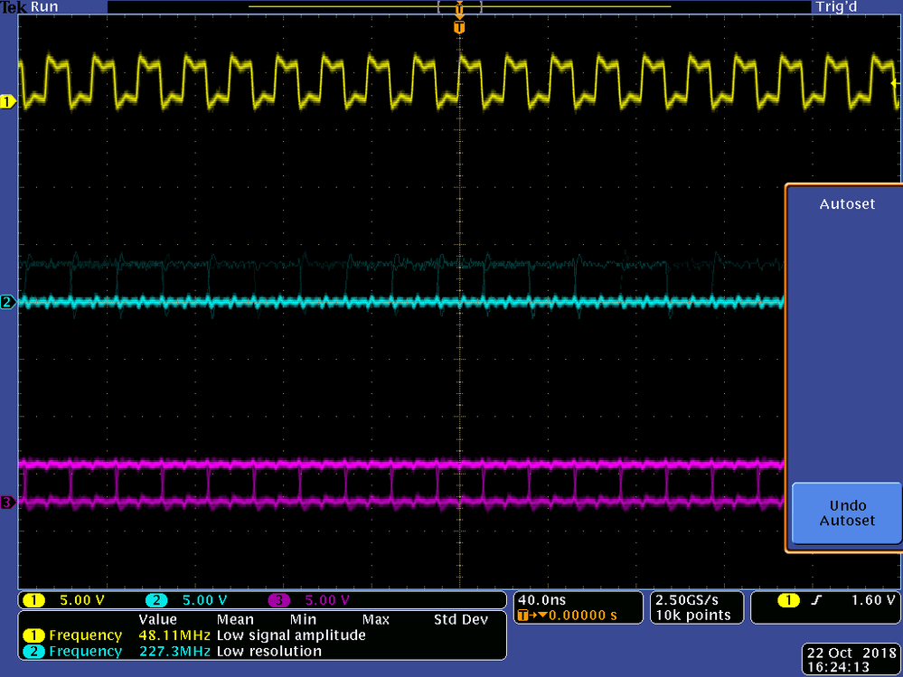
Hey @Community member I have reconsidered my options and it turns out it is necessary for me use FIFO. I decided to go for FMC as you suggested. My FIFO is synchronous so i have selected burst read write mode of PSRAM for building my FIFO controller. Since I m having a nucleo144 board with stm32f767zi , I decided to write a small test code for FMC based FIFO controller. My code has an array of type uint8_t and size 500. The content of array is like{0xFF,0x00,0xFF,0x00,0xFF,0x00,0xFF,0x00......... 500 times}. I send this to fifo using fmc and then observed the corresponding pins on oscilloscope. I expected the output to be somewhat like Fig 1 with write enable signal.
But I m not getting out as above. Please look at the following oscilloscope screenshots.
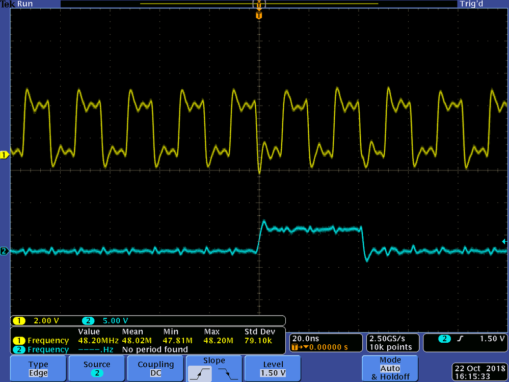
here the yellow wave is clock, My HCLK =96 MHz and FMC_CLK= HCLK/2= 48 MHz which is correct. The channel 2 (blue ) is data(only 1 bit that should go 0,1,0,1,0...and so on). It shows faint appearing and disappearing square pulses. Pink channel is Write enable signal.
My problem is when i trigger the oscilloscope for data signal and capture waves i see something like this.
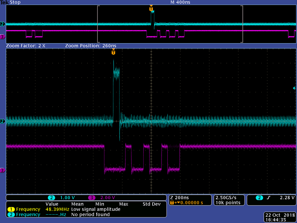
so my data bit is high for 2 FMC_CLK instead of 1 . Further when i observe Write enable signal along with data signal i see this.
since WE(write enable ) is going low and high but data is not changing so garbage values will be pussed in FIFO.
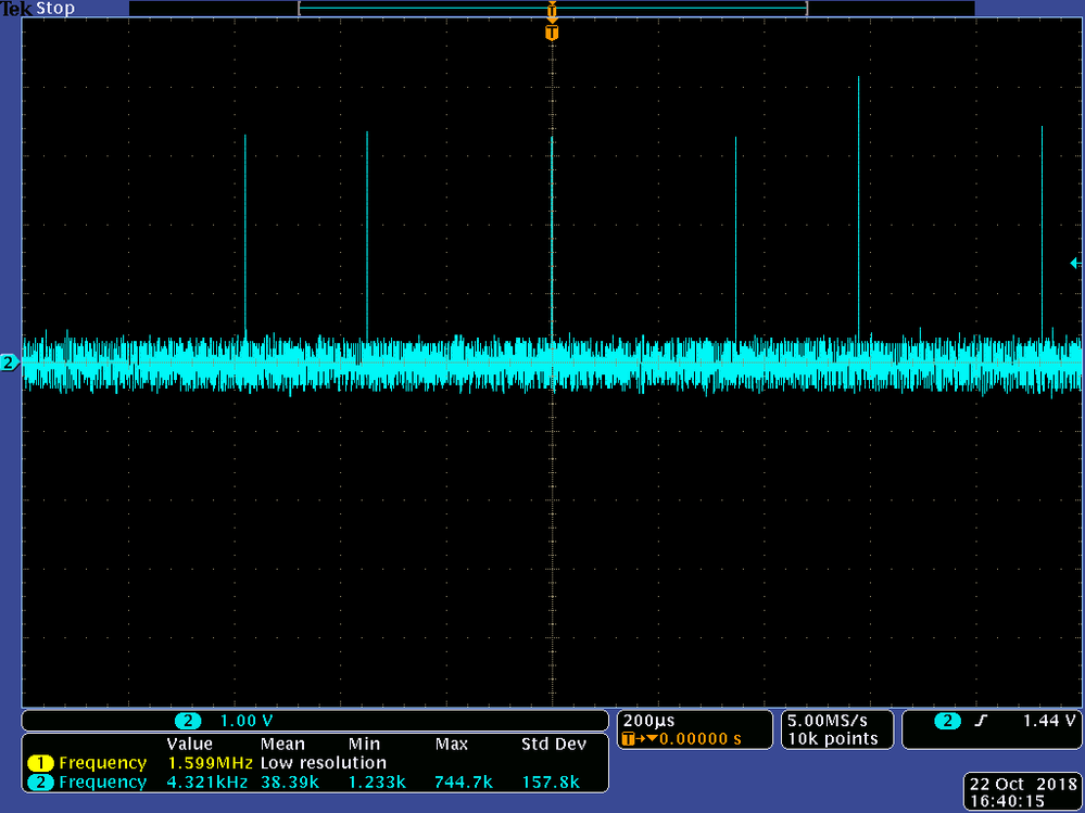
When i increase scale of oscilloscope and trigger the data signal i see this
The frequency of incoming data is very small.
Can you please have a look and help me out?
Here is my code
/* Includes ------------------------------------------------------------------*/
#include "main.h"
#include "stm32f7xx_hal.h"

/* USER CODE BEGIN Includes */
#define WRITE_READ_ADDR     ((uint32_t)0x0800)
#define BUFFER_SIZE         ((uint32_t)0x01F4)
#define SRAM_BANK_ADDR ((uint32_t)0X60000000)


/* Private variables ---------------------------------------------------------*/

SRAM_HandleTypeDef hsram1;

/* Private function prototypes -----------------------------------------------*/
void SystemClock_Config(void);
static void MX_GPIO_Init(void);
static void MX_FMC_Init(void);


int main(void)
{

  HAL_Init();


  SystemClock_Config();

  MX_GPIO_Init();
  MX_FMC_Init();

  uint8_t b[500];
   for(int i=0;i<500;i++)
   {  if(i%2==0)
		  b[i]=(uint8_t)0xFF;
	  else
		  b[i]=(uint8_t)0x00;
   }

  while (1)
  {


	  HAL_SRAM_Write_8b(&hsram1, (uint32_t *)(SRAM_BANK_ADDR + WRITE_READ_ADDR), b, BUFFER_SIZE);
	  HAL_GPIO_TogglePin(GPIOB, GPIO_PIN_14);//toggling an user LED


  }


}


void SystemClock_Config(void)
{

  RCC_OscInitTypeDef RCC_OscInitStruct;
  RCC_ClkInitTypeDef RCC_ClkInitStruct;

    /**Configure the main internal regulator output voltage
    */
  __HAL_RCC_PWR_CLK_ENABLE();

  __HAL_PWR_VOLTAGESCALING_CONFIG(PWR_REGULATOR_VOLTAGE_SCALE3);

    /**Initializes the CPU, AHB and APB busses clocks
    */
  RCC_OscInitStruct.OscillatorType = RCC_OSCILLATORTYPE_HSI;
  RCC_OscInitStruct.HSIState = RCC_HSI_ON;
  RCC_OscInitStruct.HSICalibrationValue = 16;
  RCC_OscInitStruct.PLL.PLLState = RCC_PLL_ON;
  RCC_OscInitStruct.PLL.PLLSource = RCC_PLLSOURCE_HSI;
  RCC_OscInitStruct.PLL.PLLM = 8;
  RCC_OscInitStruct.PLL.PLLN = 96;
  RCC_OscInitStruct.PLL.PLLP = RCC_PLLP_DIV2;
  RCC_OscInitStruct.PLL.PLLQ = 2;
  if (HAL_RCC_OscConfig(&RCC_OscInitStruct) != HAL_OK)
  {
    _Error_Handler(__FILE__, __LINE__);
  }

    /**Activate the Over-Drive mode
    */
  if (HAL_PWREx_EnableOverDrive() != HAL_OK)
  {
    _Error_Handler(__FILE__, __LINE__);
  }

    /**Initializes the CPU, AHB and APB busses clocks
    */
  RCC_ClkInitStruct.ClockType = RCC_CLOCKTYPE_HCLK|RCC_CLOCKTYPE_SYSCLK
                              |RCC_CLOCKTYPE_PCLK1|RCC_CLOCKTYPE_PCLK2;
  RCC_ClkInitStruct.SYSCLKSource = RCC_SYSCLKSOURCE_PLLCLK;
  RCC_ClkInitStruct.AHBCLKDivider = RCC_SYSCLK_DIV1;
  RCC_ClkInitStruct.APB1CLKDivider = RCC_HCLK_DIV2;
  RCC_ClkInitStruct.APB2CLKDivider = RCC_HCLK_DIV1;

  if (HAL_RCC_ClockConfig(&RCC_ClkInitStruct, FLASH_LATENCY_3) != HAL_OK)
  {
    _Error_Handler(__FILE__, __LINE__);
  }

    /**Configure the Systick interrupt time
    */
  HAL_SYSTICK_Config(HAL_RCC_GetHCLKFreq()/1000);

    /**Configure the Systick
    */
  HAL_SYSTICK_CLKSourceConfig(SYSTICK_CLKSOURCE_HCLK);

  /* SysTick_IRQn interrupt configuration */
  HAL_NVIC_SetPriority(SysTick_IRQn, 0, 0);
}

/* FMC initialization function */
static void MX_FMC_Init(void)
{
  FMC_NORSRAM_TimingTypeDef Timing;

  /** Perform the SRAM1 memory initialization sequence
  */
  hsram1.Instance = FMC_NORSRAM_DEVICE;
  hsram1.Extended = FMC_NORSRAM_EXTENDED_DEVICE;
  /* hsram1.Init */
  hsram1.Init.NSBank = FMC_NORSRAM_BANK1;
  hsram1.Init.DataAddressMux = FMC_DATA_ADDRESS_MUX_DISABLE;
  hsram1.Init.MemoryType = FMC_MEMORY_TYPE_PSRAM;
  hsram1.Init.MemoryDataWidth = FMC_NORSRAM_MEM_BUS_WIDTH_8;
  hsram1.Init.BurstAccessMode = FMC_BURST_ACCESS_MODE_ENABLE;
  hsram1.Init.WaitSignalPolarity = FMC_WAIT_SIGNAL_POLARITY_LOW;
  hsram1.Init.WaitSignalActive = FMC_WAIT_TIMING_BEFORE_WS;
  hsram1.Init.WriteOperation = FMC_WRITE_OPERATION_ENABLE;
  hsram1.Init.WaitSignal = FMC_WAIT_SIGNAL_DISABLE;
  hsram1.Init.ExtendedMode = FMC_EXTENDED_MODE_DISABLE;
  hsram1.Init.AsynchronousWait = FMC_ASYNCHRONOUS_WAIT_DISABLE;
  hsram1.Init.WriteBurst = FMC_WRITE_BURST_ENABLE;
  hsram1.Init.ContinuousClock = FMC_CONTINUOUS_CLOCK_SYNC_ASYNC;
  hsram1.Init.WriteFifo = FMC_WRITE_FIFO_ENABLE;
  hsram1.Init.PageSize = FMC_PAGE_SIZE_NONE;
  /* Timing */
  Timing.AddressSetupTime = 15;
   Timing.AddressHoldTime = 15;
   Timing.DataSetupTime = 255;
  Timing.BusTurnAroundDuration = 15;
  Timing.CLKDivision = 2;
  Timing.DataLatency = 2;
  Timing.AccessMode = FMC_ACCESS_MODE_A;
  /* ExtTiming */

  if (HAL_SRAM_Init(&hsram1, &Timing, NULL) != HAL_OK)
  {
    _Error_Handler(__FILE__, __LINE__);
  }

}

/** Configure pins as
        * Analog
        * Input
        * Output
        * EVENT_OUT
        * EXTI
*/
static void MX_GPIO_Init(void)
{

  GPIO_InitTypeDef GPIO_InitStruct;

  /* GPIO Ports Clock Enable */
  __HAL_RCC_GPIOE_CLK_ENABLE();
  __HAL_RCC_GPIOF_CLK_ENABLE();
  __HAL_RCC_GPIOG_CLK_ENABLE();
  __HAL_RCC_GPIOB_CLK_ENABLE();
  __HAL_RCC_GPIOD_CLK_ENABLE();
  __HAL_RCC_GPIOC_CLK_ENABLE();

  /*Configure GPIO pin Output Level */
  HAL_GPIO_WritePin(GPIOB, GPIO_PIN_14, GPIO_PIN_RESET);

  /*Configure GPIO pin : PB14 */
  GPIO_InitStruct.Pin = GPIO_PIN_14;
  GPIO_InitStruct.Mode = GPIO_MODE_OUTPUT_PP;
  GPIO_InitStruct.Pull = GPIO_NOPULL;
  GPIO_InitStruct.Speed = GPIO_SPEED_FREQ_LOW;
  HAL_GPIO_Init(GPIOB, &GPIO_InitStruct);

}
HAL_StatusTypeDef HAL_SRAM_Write_8b(SRAM_HandleTypeDef *hsram, uint32_t *pAddress, uint8_t *pSrcBuffer, uint32_t BufferSize)
{
  __IO uint8_t * psramaddress = (uint8_t *)pAddress;

  /* Check the SRAM controller state */
  if(hsram->State == HAL_SRAM_STATE_PROTECTED)
  {
    return  HAL_ERROR;
  }

  /* Process Locked */
  __HAL_LOCK(hsram);

  /* Update the SRAM controller state */
  hsram->State = HAL_SRAM_STATE_BUSY;

  /* Write data to memory */
  for(; BufferSize != 0; BufferSize--)
  {
    *(__IO uint8_t *)psramaddress = *pSrcBuffer;
    pSrcBuffer++;
    psramaddress++;
  }

  /* Update the SRAM controller state */
  hsram->State = HAL_SRAM_STATE_READY;

  /* Process unlocked */
  __HAL_UNLOCK(hsram);

  return HAL_OK;
}

/* USER CODE BEGIN 4 */

/* USER CODE END 4 */

/**
  * @brief  This function is executed in case of error occurrence.
  * @param  file: The file name as string.
  * @param  line: The line in file as a number.
  * @retval None
  */
void _Error_Handler(char *file, int line)
{
  /* USER CODE BEGIN Error_Handler_Debug */
  /* User can add his own implementation to report the HAL error return state */
  while(1)
  {
  }
  /* USER CODE END Error_Handler_Debug */
}

#ifdef  USE_FULL_ASSERT
/**
  * @brief  Reports the name of the source file and the source line number
  *         where the assert_param error has occurred.
  * @param  file: pointer to the source file name
  * @param  line: assert_param error line source number
  * @retval None
  */
void assert_failed(uint8_t* file, uint32_t line)
{
  /* USER CODE BEGIN 6 */
  /* User can add his own implementation to report the file name and line number,
     tex: printf("Wrong parameters value: file %s on line %d\r\n", file, line) */
  /* USER CODE END 6 */
}
#endif /* USE_FULL_ASSERT */
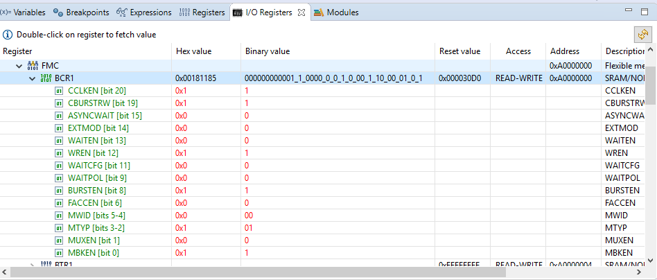
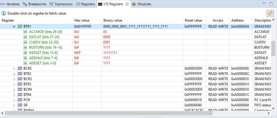
I have reffered to Ch 13 of RM0410 to check out the required configration of FMC_BCR and FMC_BTR registers. I have run my board in debug mode and checked the values of these registers. Have a look
This is the content of BCR register.
This is the content of BTR.
Please let me know what you think about it and how can this issue be resolved.
Thanks in advance.
- Mark as New
- Bookmark
- Subscribe
- Mute
- Subscribe to RSS Feed
- Permalink
- Email to a Friend
- Report Inappropriate Content
2018-10-24 3:27 AM
do you have A11 as the address strobe ?
the Ffo Address is 0x6000 0800 using A11 ?
I am confused, but thats ok...
you will learn by teaching me about your board.
in this code you have:
  /* Write data to memory */
  for(; BufferSize != 0; BufferSize--)
  {
    *(__IO uint8_t *)psramaddress = *pSrcBuffer;
    pSrcBuffer++;
    psramaddress++;
  }
it looks like you transfer your entire BufferSize..
can you see this section on the scope, its as tight as C can go. ( DMA would be faster or ASM)
this should be transfering at least 10MHz, that is max 0x1F4 length x 0.1uS = 50uS, is that about right ? on the scope ?
I glazed over your code.
I wouldn't use HAL to transfer data through the Fifo.
the snippet above /*write data to memory is all you need..
- Mark as New
- Bookmark
- Subscribe
- Mute
- Subscribe to RSS Feed
- Permalink
- Email to a Friend
- Report Inappropriate Content
2018-10-24 3:42 AM
the best way forward is to reduce the complexity.
this is untested, syntax errors abound.... just off the top of my ears
referencing your stuff:
#define WRITE_READ_ADDR     ((uint32_t)0x0800)
#define BUFFER_SIZE         ((uint32_t)0x01F4)
#define SRAM_BANK_ADDR ((uint32_t)0X60000000)

char* destPtr = SRAM_BANK_ADDR | WRITE_READ_ADDR ;

while (1){

	*destPrt = 0x50;  // write data
	*destPrt = 0x52;  // write data
	*destPrt = 0x56;  // write data
	*destPrt = 0x57;  // write data
	*destPrt = 0x5F;  // write data

	HalDelay(1);	// not sure on the syntax, I dont use delays... :(
}
This should give you a stable Scope image of 5 transactions. repeating every mS
now you should see transfers at about 40-60MHz,
that is @50MHz is 20nS per cycle, 5 cycles, is about 100nS of data, then pause for 1mS.
- Mark as New
- Bookmark
- Subscribe
- Mute
- Subscribe to RSS Feed
- Permalink
- Email to a Friend
- Report Inappropriate Content
2018-10-30 1:44 AM
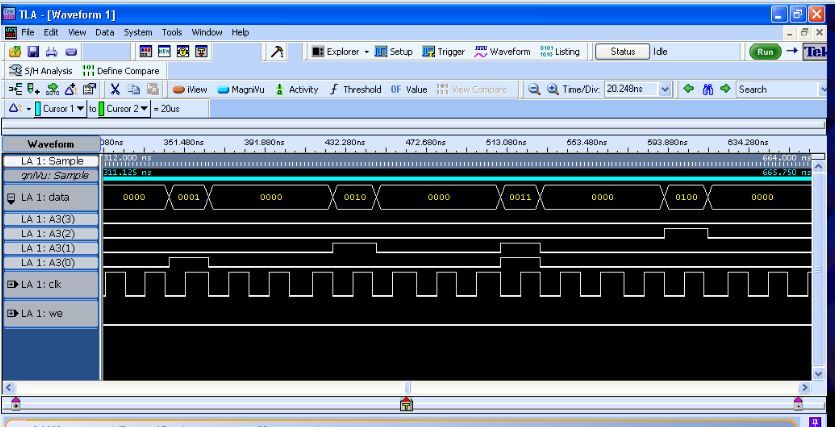
I modified my code as you suggested . Now I m sending 4 values and then waiting for 1 sec. I observed the output on logic analyser. In figure 1 i can see that data is coming in correct sequence ie 0X01,0X02,0X03,0X04.
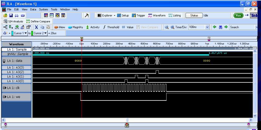
But data is not coming out at every clock and also write enable is low . See Fig 2. Data is coming once in 4 clocks.
This will lead to writing of lots of 0X00 along with required data points. How can we get one data per clock ? Or How can write enable be low only when valid data is getting outputted?
- Mark as New
- Bookmark
- Subscribe
- Mute
- Subscribe to RSS Feed
- Permalink
- Email to a Friend
- Report Inappropriate Content
2018-10-30 1:51 AM
Actually i dont need address since i want to write to a FIFO. But since i m using PSRAM controller of FMC for generating my waveforms hence i m forced to enable address. I m not clear about how all DMA channels are related to each other. Since ethernet is already using DMA. I dont want to mess with DMA here untill n unless absolutely necessary.
- Mark as New
- Bookmark
- Subscribe
- Mute
- Subscribe to RSS Feed
- Permalink
- Email to a Friend
- Report Inappropriate Content
2018-10-30 3:16 AM
good work, the data looks great on the new scope.. nice and stable.
you seem to be writing a 32bit number @ 8 bits x 4 times. hence the 4 clock strobes.
I am out of my depth when it come to casting peripherals...
please post the current code in a zip file here... I will check if I can help
- STM32F767 I2C sending byte immediately after address sent in STM32 MCUs Embedded software
- Case STM32H7 – External Flash (XIP via OctoSPI) and Large External RAM (~256MB) Interfacing Feasibility in STM32 MCUs Products
- STM32L476RG: Issue with communication between the MCU and BQ79656-Q1 AFE in STM32 MCUs Embedded software
- How to interface external watchdog STWD100 with STM32 ? in Others: STM32 MCUs related
- Interface External SRAM to extend Internal RAM at runtime in STM32CubeIDE (MCUs)

