- STMicroelectronics Community
- STM32 MCUs
- STM32 MCUs Boards and hardware tools
- STM32F7508-DK; MxCube; CN4, CN5, CN6 and CN7
- Subscribe to RSS Feed
- Mark Topic as New
- Mark Topic as Read
- Float this Topic for Current User
- Bookmark
- Subscribe
- Mute
- Printer Friendly Page
STM32F7508-DK; MxCube; CN4, CN5, CN6 and CN7
- Mark as New
- Bookmark
- Subscribe
- Mute
- Subscribe to RSS Feed
- Permalink
- Email to a Friend
- Report Inappropriate Content
2020-11-17 11:54 AM
HI, I am a beginner with STM32 but an old programmer. Bytw, my father was born in Crolles ! English is not my natural language.
I bought a development kit. I downloaded Cube MX. I create a project for this DK. But in the pinout window I can see pins that belongs to the CPU not those being in the CN4, CN5, CN6 and CN7 connectors. How can I have them ?
TIA
Jean in Grenoble (France)
Solved! Go to Solution.
- Labels:
-
STM32CubeMX
-
STM32F7 series
Accepted Solutions
- Mark as New
- Bookmark
- Subscribe
- Mute
- Subscribe to RSS Feed
- Permalink
- Email to a Friend
- Report Inappropriate Content
2020-11-17 1:41 PM
Hello @MJean.3 ,
Welcome the the STM32 Community :smiling_face_with_smiling_eyes:
In STM32CubeMx, a Pinout view shows a graphic representation of the pinout for the selected package (e.g. BGA, QFP) where each pin is represented with its name (e.g. PC4, PB8,..) and its current alternate function assignment.
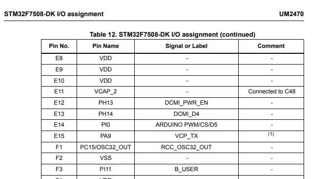
For more details on pins name and assignment of connectors (CN4, CN5, CN6 and CN7) , please refer to the UM2470.
Hope I answered your question.
If you are satisfied of my answer, please flag it as "best answer".
Imen
Thanks
Imen
- Mark as New
- Bookmark
- Subscribe
- Mute
- Subscribe to RSS Feed
- Permalink
- Email to a Friend
- Report Inappropriate Content
2020-11-17 11:43 PM
Hi Imen,
I found what I needed ! Many thanks.
If there is a wish list : I would like that Cube Mx app be able to manage Arduino connectors !
I didn't find a flag with a 'best anwer' caption. So i click on the thumb. You should be proud : it is the first time i do it ;)
Jean in Grenoble (France)
- Mark as New
- Bookmark
- Subscribe
- Mute
- Subscribe to RSS Feed
- Permalink
- Email to a Friend
- Report Inappropriate Content
2020-11-18 12:21 AM
Hi @MJean.3 ,
Glad to know you have found what you need :)
You will find the "Select as Best" flag below in my previous answer.

Imen
Thanks
Imen
- Mark as New
- Bookmark
- Subscribe
- Mute
- Subscribe to RSS Feed
- Permalink
- Email to a Friend
- Report Inappropriate Content
2020-11-20 1:27 AM
I wonder why it is so difficult to find simple information in the DK documentation !
I would like to know how can I find on which pin is connected the user button ! Where must I look for ?
I tried to find the declaration of 'gpio_pin_1' with no success (I found it in an example).
Jean
- Mark as New
- Bookmark
- Subscribe
- Mute
- Subscribe to RSS Feed
- Permalink
- Email to a Friend
- Report Inappropriate Content
2020-11-20 1:49 AM
Hi @MJean.3 ,
The specific assignments for each pin are detailed in the device datasheet: STM32F750x8 Datasheet , in the Table 10. STM32F750x8 pin and ball definition.
The user button (B_USER) is connected to the PI11.

Do you mean PJ1 pin ?

Thanks
Imen
- Mark as New
- Bookmark
- Subscribe
- Mute
- Subscribe to RSS Feed
- Permalink
- Email to a Friend
- Report Inappropriate Content
2020-11-20 3:02 AM
Hi Imen,
gpio_pin_1 is a keil problem. I ask them.
About the user push button : how can I know that its name is B_USER ?
I try to explain my problem with the reset button : in the UM2470 document, I can see on page 17 : "Reset button B2". If I search in the whole document for "B2" I can't find another occurence. But perhaps it is PB2 on page 32 : pin M5 PB2/BOOT1 ? If yes why is it not the same name ? Or if not why "B2" is not written near "J1 NRST Hardware reset" page 31 and/or on the CN6 connector page 23 ?
On the scheme page 10 under "Push_buttons", ST could have written "(user (B_user) and RESET (B2))" ...
And .... many thanks for your help !
Jean
- HardFault_Handler() after MxCube project regeneration by using ST Example project in STM32 MCUs Embedded software
- STM32N6570-DK: Missing Support for USB PHY Clock Sources in STM32CubeMX (MCUs)
- stm32cube VS Code Project Setup STM32F100 device not found in STM32CubeIDE for Visual Studio Code (MCUs)
- STM32CubeMX does not preserve conditional RTC initialization (it reinitialize when backup register is set) in STM32CubeMX (MCUs)
- Stride Value is Readonly after Update to TouchGFX 4.26 in STM32 MCUs TouchGFX and GUI