- STMicroelectronics Community
- Product forums
- Power management
- Layout Recommendation for inverting DC-DC Converte...
- Subscribe to RSS Feed
- Mark Topic as New
- Mark Topic as Read
- Float this Topic for Current User
- Bookmark
- Subscribe
- Mute
- Printer Friendly Page
Layout Recommendation for inverting DC-DC Converter MC34063
- Mark as New
- Bookmark
- Subscribe
- Mute
- Subscribe to RSS Feed
- Permalink
- Email to a Friend
- Report Inappropriate Content
2019-08-28 02:06 AM
I am using the MC34063ECD-TR to take 5V and make -12V. I'm using the schematic as recommended in the datasheet for this application (with the exception of using a 100uH inductor instead of a 90uH inductor). It is working nicely electrically - I get a pretty clean -12 Volt rail from it. The problem is I also get a loud audible hiss from the inductor. I can press on the inductor with my finger and it dampens the hissing sound. It's around 4 to 8 kHz based on my phone's FFT app, but to my ear it sounds like white noise.
Another problem is I get a lot of radiated emissions that is really messing up my analog gain stage. I have amplifiers taking a 30 kHz signal and amplifying by 110 dB (I'm taking 25uV and amplifying it to about 7.2 V). The amplification works VERY nicely under 1 of 2 conditions:
1) I depopulate the MC34063 (telling me it's either conducted or radiated emissions from the MC34063 interfering with the gain)
or
2) I cover the gain stages with a grounded metal box. (confirming it's actually 100% radiated emissions, not conducted). It's actually pretty neat - I can look at the output of the gain stages and as I cover it I can see the noise get smaller and disappear entirely.
I'm thinking this problem could be coming from a "bad layout". My question is: What pins of which parts need to be located physically close together to minimize the switching current loop for the MC34063's inverting DC-DC Converter using the datasheets recommended application schematic.
- Labels:
-
DC-DC Conversion
- Mark as New
- Bookmark
- Subscribe
- Mute
- Subscribe to RSS Feed
- Permalink
- Email to a Friend
- Report Inappropriate Content
2019-09-12 10:38 AM
Is anybody at ST able to help me with this?
- Mark as New
- Bookmark
- Subscribe
- Mute
- Subscribe to RSS Feed
- Permalink
- Email to a Friend
- Report Inappropriate Content
2019-09-12 02:17 PM
Pins 4, 5 and 2 path - short as possible.
I cant see the inner grounds to well on the views, but do see the "seperation" of the top/red layer grounds between the Inductor and C43 ground. as an experiment, try a slice of copper tape soldered in a fashion over the top of the ic, to connect the grounds together. it seems you have enough vias in some places , but i have seen a lack of just one via for an TI parts IC ground to cause it to get squirrely. worked fine on prev rev, then the via got dropped of the pcb on the next rev....sooo back to the pcb shop LOL!
another experiment maybe take a short piece of wire, solder to connect the top grounds together in the spot where the silkscreen marking is for L2 and r27 ~ area
- Mark as New
- Bookmark
- Subscribe
- Mute
- Subscribe to RSS Feed
- Permalink
- Email to a Friend
- Report Inappropriate Content
2019-09-13 05:40 AM
First let me say thank you for your suggestions! I appreciate all help I can get.
My second layer (this is a 6 layer board) is a solid ground underneath of this circuit. The slice in this screen shot is because I physically separate the amplifier and ADC circuit that is next to this regulator. Connecting a ground on top of the circuitry shouldn't help (except for covering the inductor with a shield).
- Mark as New
- Bookmark
- Subscribe
- Mute
- Subscribe to RSS Feed
- Permalink
- Email to a Friend
- Report Inappropriate Content
2019-09-13 05:51 AM
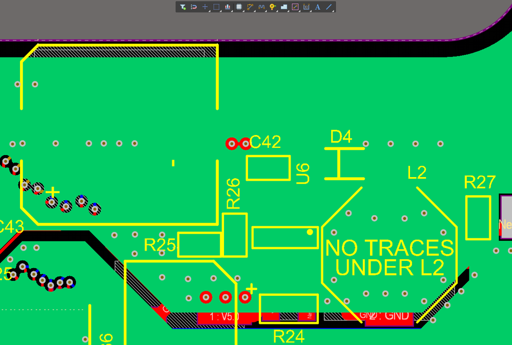
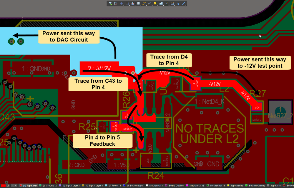
And I believe my pins 2/4/5 have very short traces, but maybe D4 could be closer to pin 4??? What do you think?
Here is how it is laid out:
- Mark as New
- Bookmark
- Subscribe
- Mute
- Subscribe to RSS Feed
- Permalink
- Email to a Friend
- Report Inappropriate Content
2019-09-13 06:01 AM
Perhaps I could flip the diode over and get it closer to pin 4. What do you think about this? Could it solve the problem?
- Information request for L6566B Vref voltage reference. in Power management
- MCU Recommendation for BMS in Hybrid Solar Inverter in STM32 MCUs Products
- Total Footprint of VIPERGAN65 based isolated AC/DC flyback converter and recommended transformer in Power management
- Can I operate a DSMPS when writing to FLASH from the MCU? in STM32 MCUs Products
- USB graceful shutdown before a software reset in STM32 MCUs Products


