- STMicroelectronics Community
- MEMS and sensors
- MEMS (sensors)
- LIS3DSH question and documentation request
- Subscribe to RSS Feed
- Mark Topic as New
- Mark Topic as Read
- Float this Topic for Current User
- Bookmark
- Subscribe
- Mute
- Printer Friendly Page
LIS3DSH question and documentation request
- Mark as New
- Bookmark
- Subscribe
- Mute
- Subscribe to RSS Feed
- Permalink
- Email to a Friend
- Report Inappropriate Content
2017-03-30 10:49 PM
I've been able to get the LIS3DSH working for single values by doing this:
transmitData[0] = (uint8_t) (LIS3DSH_READ | LIS3DSH_X_L);
SPISend( transmitData, receiveData, 2); xl = receiveData[1];But if I wanted to read out multiple values in one transaction, I'd expect that I could do something like:
transmitData[0] = (uint8_t) (LIS3DSH_READ | LIS3DSH_MULTIPLE | LIS3DSH_X_L);
transmitData[1] = (uint8_t) (LIS3DSH_READ | LIS3DSH_X_L); SPISend( transmitData, receiveData, 3); xl = receiveData[1]; xh = receiveData[2];Or have byte 2 just be 0xFF because the auto-increment would do what I expected.
But alas, it doesn't work. (yes address increment is turned on in register 6)
Can this be done? What am I missing?
Now for documentation, the temperature register just isn't documented in the data sheet. It took a while to figure out that it is Celcius and biased by -25C. Also, the M/S bit isn't documented either. I found AN3393 to be very useful, the data sheet, not so much.
Thanks,
Andrei from The Great White North.
- Labels:
-
Accelerometers
- Mark as New
- Bookmark
- Subscribe
- Mute
- Subscribe to RSS Feed
- Permalink
- Email to a Friend
- Report Inappropriate Content
2017-03-31 1:33 AM
I assume you are using 4-wire SPI interface, than you approach for multi read operation is correct. But I don't know what exactly you function SPISend does.
It would be good to check the signal with scope or logic analyzer to see if it match with the protocol.

- Mark as New
- Bookmark
- Subscribe
- Mute
- Subscribe to RSS Feed
- Permalink
- Email to a Friend
- Report Inappropriate Content
2017-03-31 9:05 AM
Sorry, yes you are correct, I'm using 4 wire SPI.
My SPISend routine is:
void
SPISend(uint8_t
* transmit,uint8_t
* receive,uint16_t
length) {HAL_StatusTypeDef
status;
HAL_GPIO_WritePin( CS_I2C_SPI_GPIO_Port, CS_I2C_SPI_Pin,
GPIO_PIN_RESET
);status = HAL_SPI_TransmitReceive( &hspi1, transmit, receive, length, 100);
HAL_GPIO_WritePin( CS_I2C_SPI_GPIO_Port, CS_I2C_SPI_Pin,
GPIO_PIN_SET
);
if
(status !=HAL_OK
) {
printf
(
''there is a problem with the transmit %d\r\n'', status);
}
}
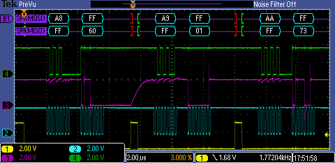
When I send two characters the pattern is:

So the signaling form is okay. At 5.25 MBaud I'm not buzzing the chip. The values that I'm getting out make sense.
I checked the wave forms on the three byte version (read | multiple | xlow, read | xhigh, dummy) and it looked good, nothing violated, but the data did not change.
Andrei
- Mark as New
- Bookmark
- Subscribe
- Mute
- Subscribe to RSS Feed
- Permalink
- Email to a Friend
- Report Inappropriate Content
2017-04-25 7:37 AM
Okay, I figured it out.
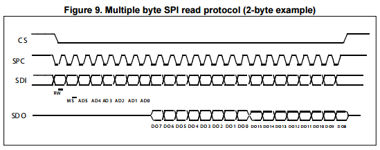
According to the timing diagram in the data sheet, bit 0x80 is the R/W bit, and 0x40 is the M/S bit, with bits 0x3F being the address bits.
In real life, there is no M/S bit. The diagram is a cut/paste from a previous generation of some other chip.
To read multiple bytes, you set the address increment bit in control 6 and just keep sending clocks.
If you set the M bit 0x40, suddenly you are just reading other registers. This device has registers in the 0x4x-0x7x range, and you just end up reading them.
So, this snippet works:
for
(uint8_t
i = 0; i < 7; i++) {transmitData[i] = 0 ;
}
transmitData[0] = (
uint8_t
) (LIS3DSH_READ |LIS3DSH_X_L);
SPISend( transmitData, receiveData, 7);
x = (
int16_t
) (receiveData[2] << 8) | (int16_t
) receiveData[1];y = (
int16_t
) (receiveData[4] << 8) | (int16_t
) receiveData[3];z = (
int16_t
) (receiveData[6] << 8) | (int16_t
) receiveData[5];So, ST, please correct your documentation. The same problem exists in the LSM6DSL documentation, and I expect many more as well.
Andrei from The Great White North
As seen on the embedded.fm podcast and blog.
- Mark as New
- Bookmark
- Subscribe
- Mute
- Subscribe to RSS Feed
- Permalink
- Email to a Friend
- Report Inappropriate Content
2017-04-25 10:23 AM
Okay, in DocID022405 Rev 2, table 15 shows the default values for register 6 being address-increment being off and watermark interrupt being on.
Section 7.7 says nothing about the default for address-increment, but has watermark interrupt being off.
If I do not set the address-increment bit, the address still increments.
I think there is something wrong with the documentation.
- Mark as New
- Bookmark
- Subscribe
- Mute
- Subscribe to RSS Feed
- Permalink
- Email to a Friend
- Report Inappropriate Content
2017-05-30 10:19 AM
I think you are right the Figures 7, 8, 9, 10, 11 in
DocID022405 Rev 2 (Datasheet for LIS3DSH)
are not correct because the bit 1 is not the M/S but is MSB of the register address. I asked sensor specialists to confirm this and fix the datasheet.I don't see this issue in the datasheet for LSM6DSL
Concerning the default value of CTRL_REG6, it is not mentioned in the table 15. I think you mistake the default value with binary representation of the register address. But you are right in the section 7.7 the default value of ADD_INC is not mentioned. This bit is set to 1 by default.
I'm sorry for the inconvenience.
- Is it necessary to perform offset calibration when measuring liquid levels with the VL53L0X? in Imaging (sensors)
- LSM6DSV16X + IIS2MDC Sensor Integration on Android 10 (i.MX8MM) in MEMS (sensors)
- LSM6DSL gyroscope and rotation order in MEMS (sensors)
- VL53L4CX: How/where to store calibration data in Imaging (sensors)
- Analog and/or digital binning with the VD55G0 CMOS sensor in Imaging (sensors)