- STMicroelectronics Community
- Automotive and Transportation
- Automotive MCUs
- Re: How to use SD2 for Serial read/write on SPC570...
- Subscribe to RSS Feed
- Mark Topic as New
- Mark Topic as Read
- Float this Topic for Current User
- Bookmark
- Subscribe
- Mute
- Printer Friendly Page
How to use SD2 for Serial read/write on SPC570S-DISP
- Mark as New
- Bookmark
- Subscribe
- Mute
- Subscribe to RSS Feed
- Permalink
- Email to a Friend
- Report Inappropriate Content
2017-12-11 05:55 PM
Hi,
I am using sample application for serial operation on SPC570S-DISP, from serial_lld.c, it looks like SD1 is mapped to LINFLEX0 and SD2 is mapped to LINFLEX1. I have no problem read/write SD1, however i need at least 2 serial port, one for console and one for API. But when i add a line of code 'sd_lld_start (&SD2, NULL); ' after the original 'sd_lld_start(&SD1, NULL);', the application stops working. Debug showing it is stuck in the first xTaskCreate (...) function call i had. If i comment out the sd_lld_start for SD2, then the xTaskCreate function call can complete and application works.
I wonder what i have missed.
I have set the SPC570Sxx Low Level Drivers Component RLA/LINFlex Settings/LINFLEX1 to Serial (default was None). I don't know if there is any other place i need to change.
Best Regards,
Job
#serialSolved! Go to Solution.
Accepted Solutions
- Mark as New
- Bookmark
- Subscribe
- Mute
- Subscribe to RSS Feed
- Permalink
- Email to a Friend
- Report Inappropriate Content
2017-12-13 05:22 PM
Hi Erwan,
I read SD1 and SD2 from RP3 by connecting the GPIO pins, i finally made it work without using the RS232 to TTL converter module. I found read from SD2 is no difference compare to read from SD1, i don't know why a RS232 to TTL converter is needed.
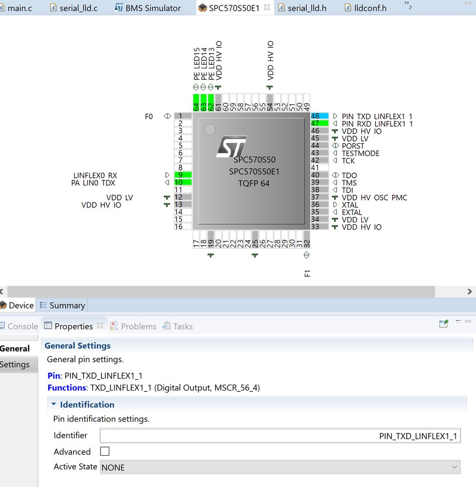
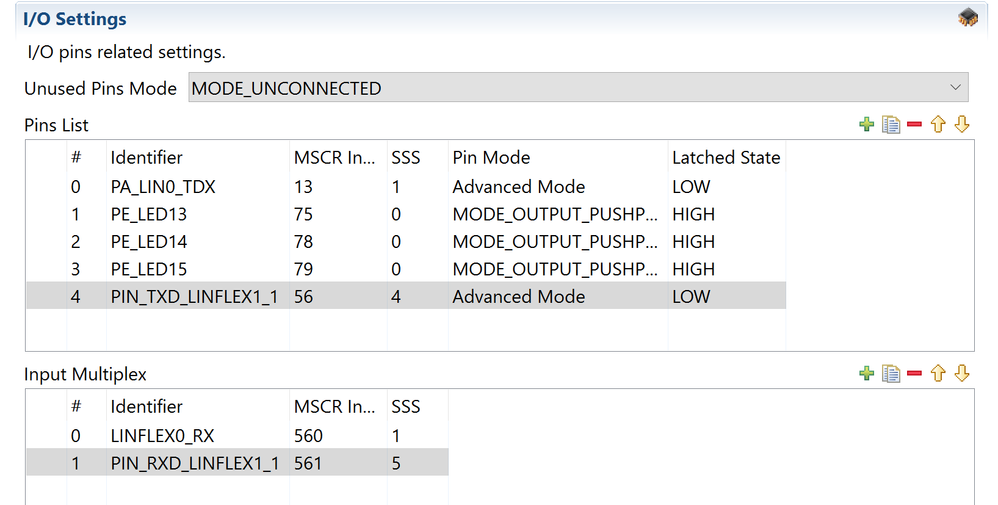
First i used pinmap editor to get the PIN name, MSCR index and function index, then i go to Board Initialization Component RLA under I/O Settings to add the entry using the PIN name, MSCR index and function index (SSS), i had no idea what MSCR and SSS is, so it took me awhile to assosicate them to the values pinmap editor properties. (i must admit it wasn't easy). I tested PIN 6 and PIN 48 for LINFLEX1 TX and both works, PIN 6 belongs to PA[8] and PIN48 belongs to PD[8].
The SPC570S-DISP board has 4 x 37 I/O pin array, using the UM2025 Hardware overview, i tried to find the corresponding pin for PD[8] for my TX,
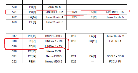
i found B21 is connected to PD[8] and C19 also connected to PD[8]. I connected to B21 and i was able to received data, but C19 has no data. When i was trying to access LINFLEX0, i found A10 had no data and C11 has data despite both connected to PA[13].
Look at below table from UM2025 Hardware overview, Page 18/24 and Page 19/24, does B21 and C19 both connected to PD[8] and should provide data?
Best Regards,
Job
- Mark as New
- Bookmark
- Subscribe
- Mute
- Subscribe to RSS Feed
- Permalink
- Email to a Friend
- Report Inappropriate Content
2017-12-12 12:47 AM
Hello Job ,
First , Did you enable LINFLEX1 Pins with the Pinmap Editor ?
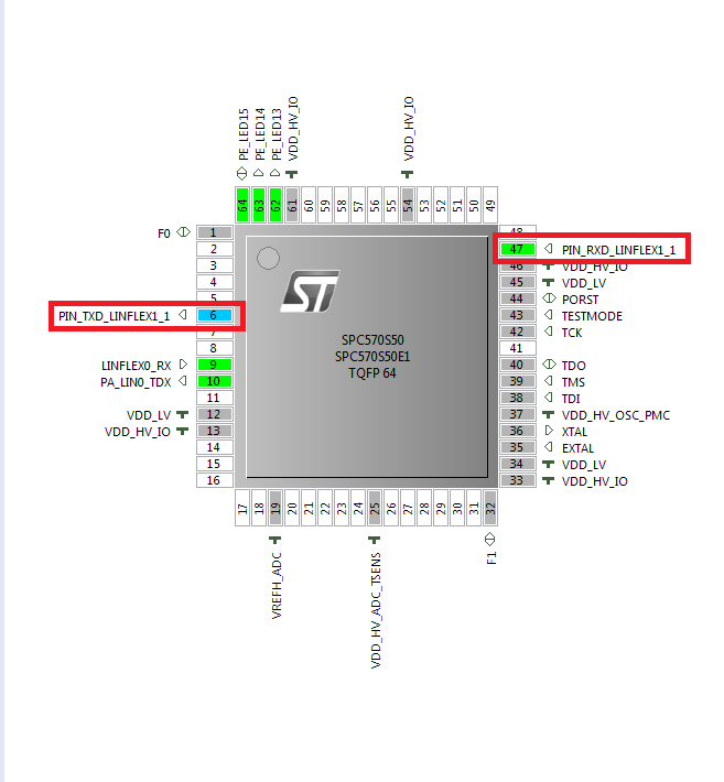
You should go in CPU Windows with PLS and check the LR in assembler mode to check where the assert is generated.
Best Regards
Erwan
- Mark as New
- Bookmark
- Subscribe
- Mute
- Subscribe to RSS Feed
- Permalink
- Email to a Friend
- Report Inappropriate Content
2017-12-12 05:49 PM
Hi Erwan,
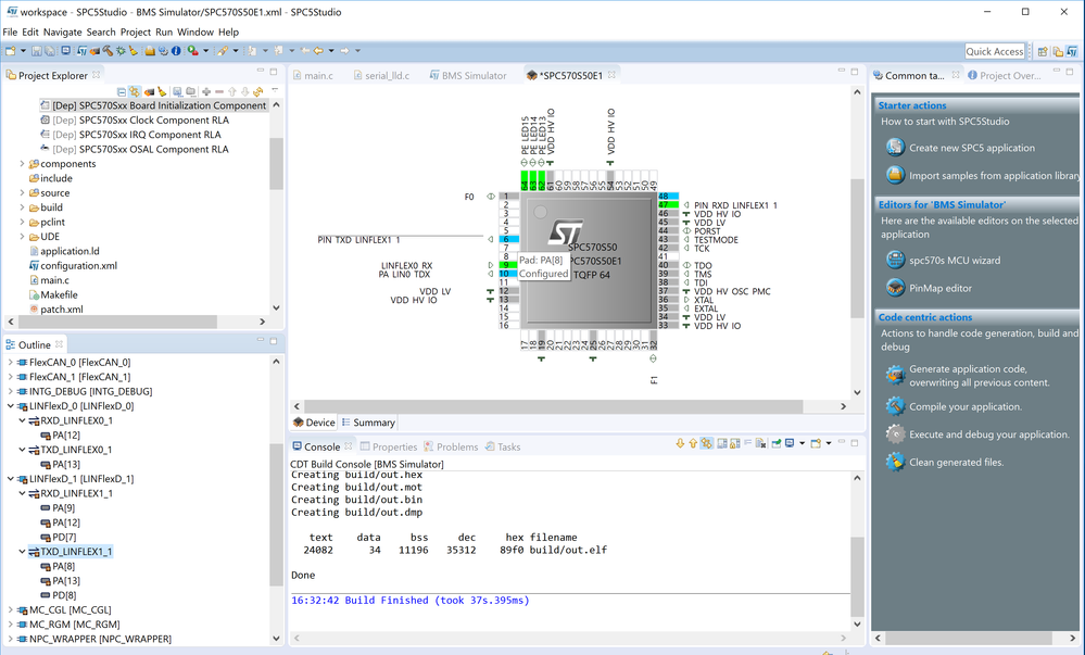
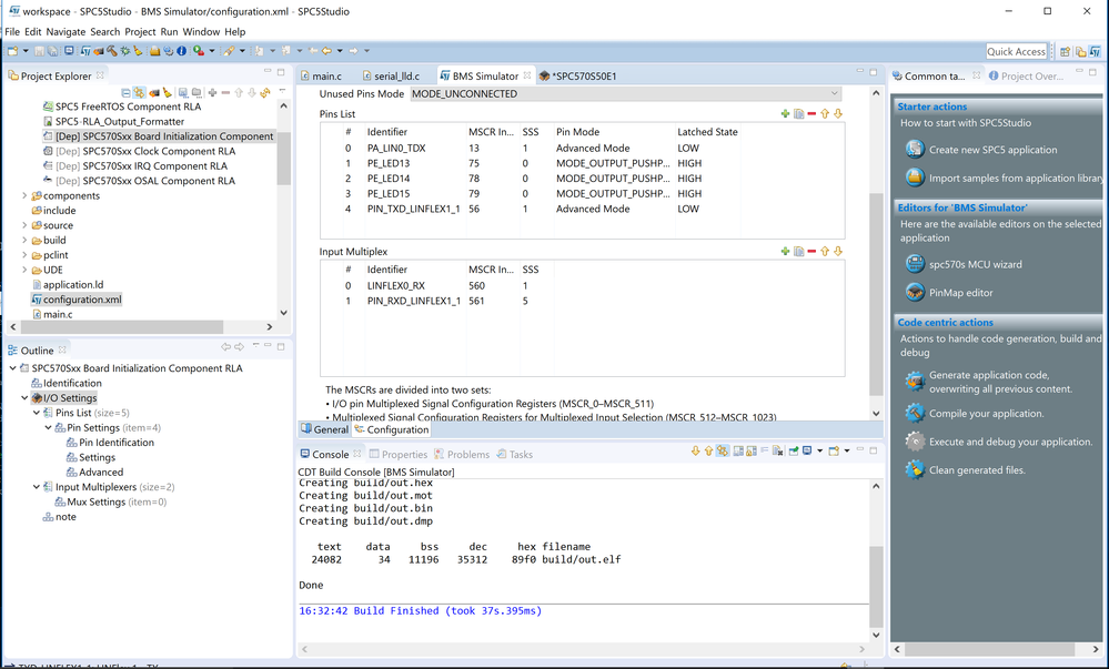
I didn't enable the LINFLEX1 with PinMap editor, thank you for pointing out that. Now that i have enabled it, the program can run, but i still not able to receive data on the LINFLEX1 TX pins when i wrote to SD2.
According to the UM2025 User Manual, the LINFLEX1-TX is mapped to PD[8], however when i use the PinMap editor, it mapped to PA[8], see attached screen shot of the mouse tip text, I was able to go to I/O settings and change the MSCR Index from 8 to 56 to make it map to PD[8]. I used same advance setting of LINFLEX0, but still not able to receive data from B21 or C19.
Anything i did wrong or overlooked?
Best Regards,
Job
- Mark as New
- Bookmark
- Subscribe
- Mute
- Subscribe to RSS Feed
- Permalink
- Email to a Friend
- Report Inappropriate Content
2017-12-13 03:28 AM
Hello Job ,
Did you try to read/write SD2 on RPI3 or PC ?
if RPI3, if directly by GPIO, you need a module
RS232 To TTL Converter Module Serial Module
We have already used LINFLEX0 (Serial PC) and LINFLEX1 (Serial => BT Device)
it works well.
Best regards
Erwan
________________ Attachments : 2331_8_6522.jpg : https://st--c.eu10.content.force.com/sfc/dist/version/download/?oid=00Db0000000YtG6&ids=0680X000006HyFz&d=%2Fa%2F0X0000000b54%2FGYkeozf76S_BG1.Zk9aH0q9t2nIYz9rFxXSn9ReLhco&asPdf=false- Mark as New
- Bookmark
- Subscribe
- Mute
- Subscribe to RSS Feed
- Permalink
- Email to a Friend
- Report Inappropriate Content
2017-12-13 05:22 PM
Hi Erwan,
I read SD1 and SD2 from RP3 by connecting the GPIO pins, i finally made it work without using the RS232 to TTL converter module. I found read from SD2 is no difference compare to read from SD1, i don't know why a RS232 to TTL converter is needed.
First i used pinmap editor to get the PIN name, MSCR index and function index, then i go to Board Initialization Component RLA under I/O Settings to add the entry using the PIN name, MSCR index and function index (SSS), i had no idea what MSCR and SSS is, so it took me awhile to assosicate them to the values pinmap editor properties. (i must admit it wasn't easy). I tested PIN 6 and PIN 48 for LINFLEX1 TX and both works, PIN 6 belongs to PA[8] and PIN48 belongs to PD[8].
The SPC570S-DISP board has 4 x 37 I/O pin array, using the UM2025 Hardware overview, i tried to find the corresponding pin for PD[8] for my TX,
i found B21 is connected to PD[8] and C19 also connected to PD[8]. I connected to B21 and i was able to received data, but C19 has no data. When i was trying to access LINFLEX0, i found A10 had no data and C11 has data despite both connected to PA[13].
Look at below table from UM2025 Hardware overview, Page 18/24 and Page 19/24, does B21 and C19 both connected to PD[8] and should provide data?


Best Regards,
Job