- STMicroelectronics Community
- Product forums
- STM8 MCUs
- TIMER 1 channels in OC mode.
- Subscribe to RSS Feed
- Mark Topic as New
- Mark Topic as Read
- Float this Topic for Current User
- Bookmark
- Subscribe
- Mute
- Printer Friendly Page
TIMER 1 channels in OC mode.
- Mark as New
- Bookmark
- Subscribe
- Mute
- Subscribe to RSS Feed
- Permalink
- Email to a Friend
- Report Inappropriate Content
2019-08-31 05:27 AM

/* My own code */

#include "STM8S.h"


void clock_setup(void);
void GPIO_setup(void);
void TIM1_setup(void);


void main(void)
{
	// signed int i = 0;

	clock_setup();
	GPIO_setup();
	TIM1_setup();

	/* Duty Cycle varied continuously to alter the blinking rate of LEDs
	while(TRUE)
	{
		for(i = 0; i < 1000; i += 1)
		{
			TIM1_SetCompare1(i);
			delay_ms(1);
		}
		for(i = 1000; i > 0; i -= 1)
		{
			TIM1_SetCompare1(i);
			delay_ms(1);
		}
	}; */
}


void clock_setup(void)
{
	CLK_DeInit();

	CLK_HSECmd(DISABLE);
	CLK_LSICmd(DISABLE);
	CLK_HSICmd(ENABLE);
	while(CLK_GetFlagStatus(CLK_FLAG_HSIRDY) == FALSE);

	CLK_ClockSwitchCmd(ENABLE);
	CLK_HSIPrescalerConfig(CLK_PRESCALER_HSIDIV1);
	CLK_SYSCLKConfig(CLK_PRESCALER_CPUDIV1);

	CLK_ClockSwitchConfig(CLK_SWITCHMODE_AUTO, CLK_SOURCE_HSI,
	DISABLE, CLK_CURRENTCLOCKSTATE_ENABLE);

	CLK_PeripheralClockConfig(CLK_PERIPHERAL_I2C, DISABLE);
	CLK_PeripheralClockConfig(CLK_PERIPHERAL_SPI, DISABLE);
	CLK_PeripheralClockConfig(CLK_PERIPHERAL_ADC, DISABLE);
	CLK_PeripheralClockConfig(CLK_PERIPHERAL_AWU, DISABLE);
	CLK_PeripheralClockConfig(CLK_PERIPHERAL_UART1, DISABLE);
	CLK_PeripheralClockConfig(CLK_PERIPHERAL_TIMER1, ENABLE);
	CLK_PeripheralClockConfig(CLK_PERIPHERAL_TIMER2, DISABLE);
	CLK_PeripheralClockConfig(CLK_PERIPHERAL_TIMER4, DISABLE);
}


void GPIO_setup(void)

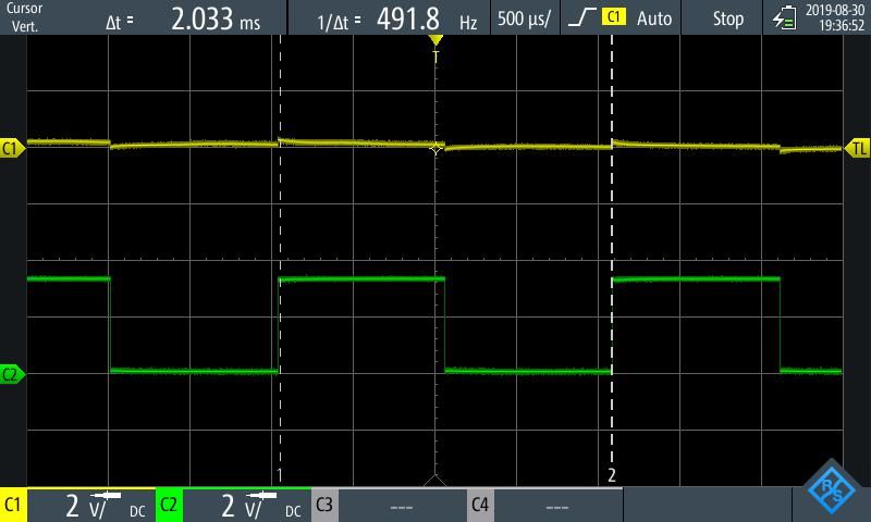
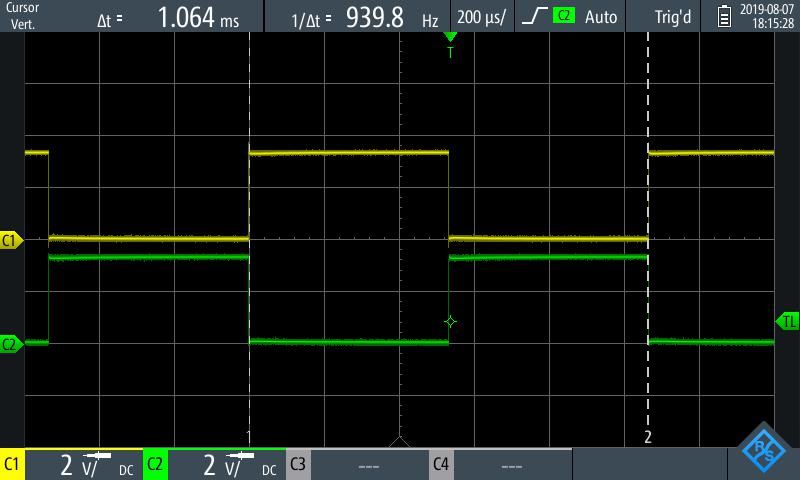
 /*TIM1_CH2 & CH2N configured in OC Mode. On executing the code, complementary PWM signals are seen on the scope. Other channels can be configured in the same way, however CH1 and CH3 pins produce no outputs */
{
	GPIO_DeInit(GPIOB);
	GPIO_Init(GPIOB, GPIO_PIN_1, GPIO_MODE_OUT_PP_HIGH_FAST);  /* Port B Pin 1 or TIM1_CH2N gets configured in the OC mode */

	GPIO_DeInit(GPIOC);
	GPIO_Init(GPIOC, GPIO_PIN_2, GPIO_MODE_OUT_PP_HIGH_FAST); /* Port C Pin 2 or TIM1_CH2 gets configured in the OC mode */
}


void TIM1_setup(void)
{
	TIM1_DeInit();

	TIM1_TimeBaseInit(16, TIM1_COUNTERMODE_UP, 1000, 1);

	TIM1_OC2Init(TIM1_OCMODE_PWM1,
							TIM1_OUTPUTSTATE_ENABLE,
						        TIM1_OUTPUTNSTATE_ENABLE,
							500,
							TIM1_OCPOLARITY_LOW,
							TIM1_OCNPOLARITY_LOW,
							TIM1_OCIDLESTATE_RESET,
							TIM1_OCNIDLESTATE_RESET);  /*TIM1_CH2 & CH2N setup.
                                             PWM output of 1 kHz frequency and 50% duty cycle obtained */

	TIM1_CtrlPWMOutputs(ENABLE);
	TIM1_Cmd(ENABLE);
}- Questions about the SAR ADC channels and configurations for our application in STM32 MCUs Products
- stm32h503 how read multi channel value in interrupt mode in STM32 MCUs Products
- Strange issue with timer pwm in dma mode in STM32 MCUs Products
- ADC mutli channel, DMA odd behaviour in STM32 MCUs Embedded software
- Can all selected channel's sampling in each SAR ADC(0-2) be trigged by the same timer so that their samples can be synchronized ? in STM32 MCUs Products
