- STMicroelectronics Community
- STM32 MPUs
- STM32 MPUs Products and hardware related
- Low Power Application Question
- Subscribe to RSS Feed
- Mark Topic as New
- Mark Topic as Read
- Float this Topic for Current User
- Bookmark
- Subscribe
- Mute
- Printer Friendly Page
Low Power Application Question
- Mark as New
- Bookmark
- Subscribe
- Mute
- Subscribe to RSS Feed
- Permalink
- Email to a Friend
- Report Inappropriate Content
2021-03-19 1:43 PM
Hello everyone!
I had an application that was originally designed to run on a STM32WB55 but found it didn't have the resources we needed for it. The STM32MP1 seems like it has the potential to be a good fit for us as we could do the sensor processing on the M4 and some of the higher level calculations on the A7.
Our plan was to have the chip asleep until it received a wakeup signal from a sensor and then most the code was running from the M4. Once it had completed its data collection, it would do the processing from the A7.
We're still in the planning phase (to determine if this is the right processor for this application) but the issue I'm having trouble navigating is the low power modes. Below are some of the questions I have:
1) If I'm having code running on the M4, is it possible to put the A7 into a low power mode (like standby or stop)? I believe this would be possible according to page 134 of the datasheet (which seems to show this capability).
2) What is the recommended mode to run on the A7 so that I don't need to boot the system from scratch on wakeup? Or would all of the modes be able to wake up and resume? Is this what the "data retention" refers to?
3) Is it possible to wakeup only the M4 core rather than the A7 or does the A7 core have to be woken up to wake the M4?
Any help you can give me would be greatly appreciated. Thanks!
- Labels:
-
STM32MP15 Lines
- Mark as New
- Bookmark
- Subscribe
- Mute
- Subscribe to RSS Feed
- Permalink
- Email to a Friend
- Report Inappropriate Content
2021-03-22 1:02 AM
Hi,
Note that the capabilities are linked to HW, but also to Linux SW. I think for your case, you could use LPLV-Stop, which ensure fast M4 wakeup from GPIO/EXTI while having minimal power from Linux. If power is a concern, Standby is possible, but with more constrains (e.g. longer wakeup times, Only RETRAM retained for M4, need to use WKUP pins).
Note that in all cases, the DDR power in self-refresh must be added in your platform power (as well as all external components as usual).
I recommend that you start by reading https://wiki.st.com/stm32mpu/wiki/How_to_define_your_low-power_strategy.
You could probably find many useful data in the other wiki pages.
Regards.
NEW ! Sidekick STM32 AI agent, see here
- Mark as New
- Bookmark
- Subscribe
- Mute
- Subscribe to RSS Feed
- Permalink
- Email to a Friend
- Report Inappropriate Content
2021-03-22 3:55 PM
This is a great page, hadn't seen that one before! I'll have to read some of the other pages linked, seems like there's a lot of good info here! So, if I am reading this correctly:
1) Each of the modes mentioned don't require a cold boot and it is able to wake up from these states without the 30s bootup time that normally comes with booting linux?
2) It sounds like the RETRAM is specific to the M4? If so, that makes sense (and seems to be what this page suggests).
One additional question I had had more to do with the RAM itself (let me know if I should open a separate ticket). The description of the RAM was a bit more complicated than that of the STM32WB55 (which makes sense as this has a uC and a uP sharing resources). It describes the RAM situation of the STM32MP157A (which is what is used with the DK1 board, which is what we'll be starting with) as:
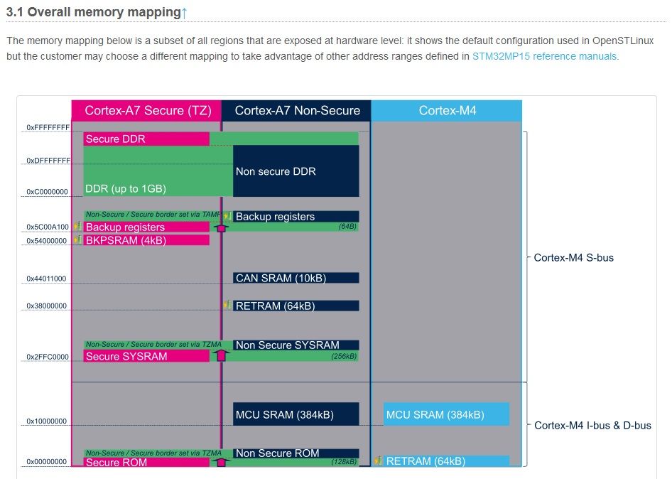
708 Kbytes of internal SRAM: 256 Kbytes of AXI SYSRAM + 384 Kbytes of AHB SRAM + 64 Kbytes of AHB SRAM in Backup domain and 4 Kbytes of SRAM in Backup domain
It was harder for me to understand what will be available for the M4 (where most our processing will be). I decided to build a simple project and take a look at the resources available (to make sure we have at least 256 kb of RAm to work with so we can port a good chunk of code over from the WB55. When I looked at the resources available, i was a bit confused:

I was able to find this on that page you sent me (once again, thanks for that, great reference!)

I apologize if these are really basic questions, this is my first time using a chip with a coprocessor and shared resources.
Thanks for your help!
- Mark as New
- Bookmark
- Subscribe
- Mute
- Subscribe to RSS Feed
- Permalink
- Email to a Friend
- Report Inappropriate Content
2021-03-23 2:28 AM
Hi, you already find most of your information.
On OpenSTLInux, SYSRAM and DDR are reserved for A7 side,
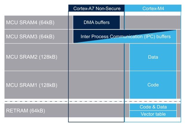
For Cortex-M4, you have 384K+64K available for code, constant and data.
see https://wiki.st.com/stm32mpu/wiki/STM32MP15_RAM_mapping#Zoom_in_the_Cortex-A7-2FCortex-M4_shared_memory for details, as some areas could be reserved for Linux DMA buffers and Interprocess buffers.
"xx_text" is your code/constant area (mostly SRAM1/SRAM2), and "***_ipc_shm" is the interprocess buffers, see also https://wiki.st.com/stm32mpu/wiki/Linux_RPMsg_framework_overview
Regards.
NEW ! Sidekick STM32 AI agent, see here
- Mark as New
- Bookmark
- Subscribe
- Mute
- Subscribe to RSS Feed
- Permalink
- Email to a Friend
- Report Inappropriate Content
2021-03-23 11:25 AM
Ah, I must've missed that page! Well, looks like the pieces are coming together a bit now. So, if I follow those pages, it's default setup with 128kB in SRAM2 for variables and such, and 128kB in SRAM1 for code space.

It looks like I can reconfigure it (in the linux device tree and the M4 linker file) so I can allocate the 256 kB in however I want between the two of them (so if I want 2 kB of variables and the remaining 254 kB into code space, I would set SRAM2 to 2 kB and 254kB in SRAM1), correct?
The RETRAM I'm a bit less clear on how that's configured. It appears you can move the vector start section so if you had 2 kB, you could potentially move the location to the last 2 kB, which leaves the 62 kB left for code and data? If so, how do you configure that? Similar to the way you setup SRAM1 and SRAM2.
Related question, is there a way to differentiate between data (variables) and flash (code space) in RAM or does the compiler itself know how to manage that? I'm looking at the linker code (for instance) and I see that it has the starting location and the length but I don't really see how it separates variables and code space (or if it even needs to).
Sorry if these are really basic questions, I've been able to follow directions in other projects regarding how to do it with the WB55, for instance, but I don't really know what happens behind the scenes to organize the memory between variables and code space.
Thanks again for all the help!
- Mark as New
- Bookmark
- Subscribe
- Mute
- Subscribe to RSS Feed
- Permalink
- Email to a Friend
- Report Inappropriate Content
2021-03-23 11:40 AM
I might have answered part of the question but it does potentially cause more confusion for me with the labels.
Below is the default values:
/* Memories definition */
MEMORY
{
  RETRAM_interrupts		(xrw)	: ORIGIN = 0x00000000,	LENGTH = 0x00000298
  FLASH_text		(rx)	: ORIGIN = 0x10000000,	LENGTH = 128K
  RAM1_data		(xrw)	: ORIGIN = 0x10020000,	LENGTH = 128K
  RAM2_ipc_shm		(xrw)	: ORIGIN = 0x10040000,	LENGTH = 0x00008000
}
Appears to be 128 kB for code space (which I assume is SRAM1, described as Flash_text).
Appears to have 128 kB for variables (which I assume is SRAM2, described as RAM1_data).
It seems to have 32 kB of IPC buffers in the SRAM3 section (described as RAM2_ipc_shm).
So now I'm confused with the labels, which appear to be inconsistent with the chart, unless I have a fundamental understanding issue, which seems more likely.
But, if my assumptions are correct and I want, say, 192 kB of flash/code and 64 kB of variables/data, I assume I'd change it to the following:
/* Memories definition */
MEMORY
{
  RETRAM_interrupts		(xrw)	: ORIGIN = 0x00000000,	LENGTH = 0x00000298
  FLASH_text		(rx)	: ORIGIN = 0x10000000,	LENGTH = 192K
  RAM1_data		(xrw)	: ORIGIN = 0x10030000,	LENGTH = 64K
  RAM2_ipc_shm		(xrw)	: ORIGIN = 0x10040000,	LENGTH = 0x00008000
}
If this is the case, I'm not entirely sure how/where the additional code space in RETRAM (and where it ends and the interrupt vectors begin). I might be way off, still trying to make sure I understand how all this works.
Thanks again for all your help!
- STM32MP157C: boot hangs after listing clocks in STM32 MPUs Embedded software and solutions
- Secure Application in stm32mp257-DK in STM32 MPUs Products and hardware related
- Issue with I3C4 Communication on STM32MP257F-EV1 with LSM6DSV Device in STM32 MPUs Products and hardware related
- ISP IQTune tool not working in STM32 MPUs Products and hardware related
- Learning Path suggestion in STM32 MPUs Products and hardware related