Turn on suggestions
Auto-suggest helps you quickly narrow down your search results by suggesting possible matches as you type.
Showing results for
- STMicroelectronics Community
- STM32 MCUs
- STM32 MCUs Products
- the problem of STM32F439 about the LCD_FRAME_BUFFE...
Options
- Subscribe to RSS Feed
- Mark Topic as New
- Mark Topic as Read
- Float this Topic for Current User
- Bookmark
- Subscribe
- Mute
- Printer Friendly Page
the problem of STM32F439 about the LCD_FRAME_BUFFER
Options
- Mark as New
- Bookmark
- Subscribe
- Mute
- Subscribe to RSS Feed
- Permalink
- Email to a Friend
- Report Inappropriate Content
2013-05-02 08:45 PM
Posted on May 03, 2013 at 05:45 i can't understand.can you help me ? Thank you very much?the board is the eval .the mcu is STM32F439. ROY aizhixi@gmail.com
hello, i have a eval board of STM32F439.i have some problems.
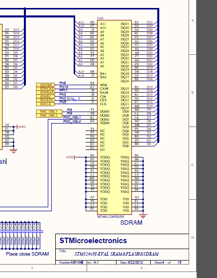
the first one:when i used the LCD-TFT Controller to display the LCD,I found the demo have a code of #define LCD_FRAME_BUFFER ((uint32_t)0xC0000000)#define BUFFER_OFFSET ((uint32_t)0x130000)i don't know why ,where i can found ,it should be the address,right?but i don't know how to get it?In the data sheet is LTDC Layerx Color Frame Buffer Address Register (LTDC_LxCFBAR),This register defines the color frame buffer start address which has to point to the address, where the pixel data of the top left pixel of a layer is stored in the frame buffer.why the address 0xc000000 ,not the others,i change the address,i found it can't display。the BUFFER_OFFSET ((uint32_t)0x130000),why ?the second :/* Internal Buffer defined in SDRAM memory */uint32_t uwInternelBuffer = 0xC0260000;that why? i don't know why the SDRAM address is 0xC0260000,i change it,but have some problems. i can't understand.can you help me ? Thank you very much?the board is the eval .the mcu is STM32F439. ROY aizhixi@gmail.com
2 REPLIES 2
Options
- Mark as New
- Bookmark
- Subscribe
- Mute
- Subscribe to RSS Feed
- Permalink
- Email to a Friend
- Report Inappropriate Content
2013-05-03 06:38 AM
Posted on May 03, 2013 at 15:38
This material is all likely under NDA, you perhaps should be discussing it privately with your ST contacts and FAE.
The base address of SDRAM is likely 0xC0000000, the frame buffer is an offset in 16-bit words, and allows you to carve out a buffer from your own floor-planing of the SDRAM usage, and expressed coherently to the LCD controller.
Tips, Buy me a coffee, or three.. PayPal Venmo
Up vote any posts that you find helpful, it shows what's working..
Up vote any posts that you find helpful, it shows what's working..
Options
- Mark as New
- Bookmark
- Subscribe
- Mute
- Subscribe to RSS Feed
- Permalink
- Email to a Friend
- Report Inappropriate Content
2013-05-03 07:28 AM
Posted on May 03, 2013 at 16:28
As Clive states, address 0xc000000 likely enables the CS pin of that SDRAM. Pin PH3 (MCU) is shown tied to that Ram CS - thus the relationship between 0xc000000 and PH3 (not intuitive to this reporter) must be discovered. Probing CS (via scope) of that Ram while generating address 0xc000000 will further illuminate.
Note that the 2 buffer addresses have a 2:1 ratio - suggests that one holds frame-buffer and the 2nd better enables ''collision-free'' fills of the frame - which may then be ''ping-ponged.'' Likely that the range of both Ram buffers are equal... Again - as Clive states - should you modify any demo ''defaults'' you must better understand how the Ram is mapped - and avoid over-writes of any/all critical sectors...
Related Content
- Two Serial ports with HAL_UARTEx_RxEventCallback don't work for me in STM32 MCUs Products
- MJPEG Video Decoding (stm32h747I) in STM32 MCUs Products
- Problem with initialization of MX_DMA2D_Init() - Camera and LCD screen in STM32 MCUs TouchGFX and GUI
- STM32H743 SAI DMA noise in STM32 MCUs Products
- TCP Server receives proper data but shows incorrect received data length in STM32F439 in STM32 MCUs Products