- STMicroelectronics Community
- STM32 MCUs
- STM32 MCUs Products
- STM32F756 Alternate function
- Subscribe to RSS Feed
- Mark Topic as New
- Mark Topic as Read
- Float this Topic for Current User
- Bookmark
- Subscribe
- Mute
- Printer Friendly Page
STM32F756 Alternate function
- Mark as New
- Bookmark
- Subscribe
- Mute
- Subscribe to RSS Feed
- Permalink
- Email to a Friend
- Report Inappropriate Content
2023-09-07 8:26 AM
Hi there, i come across AN4760 p55, configuring GPIOB with alternate functions :
GPIOB->AFR[0] = 0x0A000900; where does this 0A000900 come to config PB2 n PB6 to QSPI alternate function?
GPIOB->AFR[1] = 0x00000000;
....
GPIOF->AFR[0] |= 0x9900000000; how this 9900000000 set to config PF6, PF7 PF8 PF9 to QSPI alt. function?
GPIOF->AFR[1] |= 0x000000AA
Pls advise...thx.
Solved! Go to Solution.
- Labels:
-
STM32F7 series
Accepted Solutions
- Mark as New
- Bookmark
- Subscribe
- Mute
- Subscribe to RSS Feed
- Permalink
- Email to a Friend
- Report Inappropriate Content
2023-09-08 7:43 AM
Hello @StanJerm ,
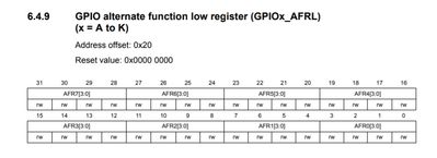
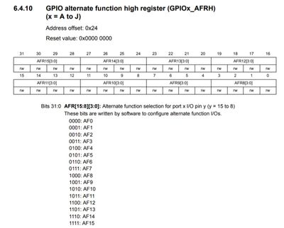
When you refer to RM0385 as already mentioned by @Issamos , the configuration of alternative function of PB2, PB6, PF6, PF7, PF7 and PF8 are made in GPIOx_AFRL (GPIOx->AFR[0]) and in GPIOx_AFRH (GPIOx->AFR[1]).
In this case:
-GPIOB configuration is done by:
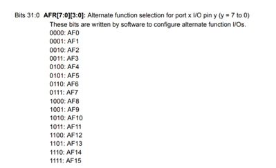
- GPIOB->AFR[0] = 0x0A000900; is used to configure PB2 and PB6 to QSPI alternate function AF9 and AF10 respectively as shown in the below table:
|
GPIOB |
||||||||
|
PB pins |
PB7 |
PB6 |
PB5 |
PB4 |
PB3 |
PB2 |
PB1 |
PB0 |
|
AFR[0] |
0 |
A |
0 |
0 |
0 |
9 |
0 |
0 |
|
0000 |
1010 |
0000 |
0000 |
0000 |
1001 |
0000 |
0000 |
|
|
Alternate Function |
AF0 |
AF10 |
AF0 |
AF0 |
AF0 |
AF9 |
AF0 |
AF0 |
- GPIOB->AFR[1] = 0x00000000;
|
GPIOB |
||||||||
|
PB pins |
PB15 |
PB14 |
PB13 |
PB12 |
PB11 |
PB10 |
PB9 |
PB8 |
|
AFR[1] |
0 |
0 |
0 |
0 |
0 |
0 |
0 |
0 |
|
0000 |
0000 |
0000 |
0000 |
0000 |
0000 |
0000 |
0000 |
|
|
Alternate Function |
AF0 |
AF0 |
AF0 |
AF0 |
AF0 |
AF0 |
AF0 |
AF0 |
-GPIOF configuration is done by:
- GPIOF->AFR[0] |= 0x99000000; is used to configure PF6 and PF7 to QSPI alternate function AF9 as shown in the below table:
|
GPIOF |
||||||||
|
PF pins |
PF7 |
PF6 |
PF5 |
PF4 |
PF3 |
PF2 |
PF1 |
PF0 |
|
AFR[0] |
9 |
9 |
0 |
0 |
0 |
0 |
0 |
0 |
|
1001 |
1001 |
0000 |
0000 |
0000 |
0000 |
0000 |
0000 |
|
|
Alternate Function |
AF9 |
AF9 |
AF0 |
AF0 |
AF0 |
AF0 |
AF0 |
AF0 |
- GPIOF->AFR[1] |= 0x000000AA ; is used to configure PF8 and PF9 to QSPI alternate function AF10 as shown in the below table:
|
GPIOF |
||||||||
|
PF pins |
PF15 |
PF14 |
PF13 |
PF12 |
PF11 |
PF10 |
PF9 |
PF8 |
|
AFR[0] |
0 |
0 |
0 |
0 |
0 |
0 |
A |
A |
|
0000 |
0000 |
0000 |
0000 |
0000 |
0000 |
1010 |
1010 |
|
|
Alternate Function |
AF0 |
AF0 |
AF0 |
AF0 |
AF0 |
AF0 |
AF10 |
AF10 |
Thank you.
Kaouthar
To give better visibility on the answered topics, please click on Accept as Solution on the reply which solved your issue or answered your question.
- Mark as New
- Bookmark
- Subscribe
- Mute
- Subscribe to RSS Feed
- Permalink
- Email to a Friend
- Report Inappropriate Content
2023-09-07 9:09 AM - edited 2023-09-07 9:13 AM
Hello @StanJerm
The board and the quad-spi flash memory are connected like this:
Then we have to programme every pin to the alternate function that it should be using. Taking a look to the DocID027589 Rev 4 (datasheet of the STM32F756) we find out that PB2, PF6 and PF7 should be configured to AF9 and PB6, PF8 and PF9 should be configured to AF10. Then and using the GPIO alternate function low register (GPIOx_AFRL) and GPIO alternate function high register (GPIOx_AFRH) we have to do this configuration. Wish is the same as the Alternate function configuration in the AN4760. ( have a look at RM0385)
best regards.
II
- Mark as New
- Bookmark
- Subscribe
- Mute
- Subscribe to RSS Feed
- Permalink
- Email to a Friend
- Report Inappropriate Content
2023-09-07 9:17 AM
Sorry, got no familiarity with your code or situation. Maybe you can expand on the detail so we understand the context better?
Often configured via Cube MSP code, or HAL GPIO Init functions. Can be a hold-over from external loaders or debug scripts, or boot loader, if they are bringing up the board.
Generally you'd want to mask on new settings, ORing tends to presume the original content is zero
Up vote any posts that you find helpful, it shows what's working..
- Mark as New
- Bookmark
- Subscribe
- Mute
- Subscribe to RSS Feed
- Permalink
- Email to a Friend
- Report Inappropriate Content
2023-09-08 7:43 AM
Hello @StanJerm ,
When you refer to RM0385 as already mentioned by @Issamos , the configuration of alternative function of PB2, PB6, PF6, PF7, PF7 and PF8 are made in GPIOx_AFRL (GPIOx->AFR[0]) and in GPIOx_AFRH (GPIOx->AFR[1]).
In this case:
-GPIOB configuration is done by:
- GPIOB->AFR[0] = 0x0A000900; is used to configure PB2 and PB6 to QSPI alternate function AF9 and AF10 respectively as shown in the below table:
|
GPIOB |
||||||||
|
PB pins |
PB7 |
PB6 |
PB5 |
PB4 |
PB3 |
PB2 |
PB1 |
PB0 |
|
AFR[0] |
0 |
A |
0 |
0 |
0 |
9 |
0 |
0 |
|
0000 |
1010 |
0000 |
0000 |
0000 |
1001 |
0000 |
0000 |
|
|
Alternate Function |
AF0 |
AF10 |
AF0 |
AF0 |
AF0 |
AF9 |
AF0 |
AF0 |
- GPIOB->AFR[1] = 0x00000000;
|
GPIOB |
||||||||
|
PB pins |
PB15 |
PB14 |
PB13 |
PB12 |
PB11 |
PB10 |
PB9 |
PB8 |
|
AFR[1] |
0 |
0 |
0 |
0 |
0 |
0 |
0 |
0 |
|
0000 |
0000 |
0000 |
0000 |
0000 |
0000 |
0000 |
0000 |
|
|
Alternate Function |
AF0 |
AF0 |
AF0 |
AF0 |
AF0 |
AF0 |
AF0 |
AF0 |
-GPIOF configuration is done by:
- GPIOF->AFR[0] |= 0x99000000; is used to configure PF6 and PF7 to QSPI alternate function AF9 as shown in the below table:
|
GPIOF |
||||||||
|
PF pins |
PF7 |
PF6 |
PF5 |
PF4 |
PF3 |
PF2 |
PF1 |
PF0 |
|
AFR[0] |
9 |
9 |
0 |
0 |
0 |
0 |
0 |
0 |
|
1001 |
1001 |
0000 |
0000 |
0000 |
0000 |
0000 |
0000 |
|
|
Alternate Function |
AF9 |
AF9 |
AF0 |
AF0 |
AF0 |
AF0 |
AF0 |
AF0 |
- GPIOF->AFR[1] |= 0x000000AA ; is used to configure PF8 and PF9 to QSPI alternate function AF10 as shown in the below table:
|
GPIOF |
||||||||
|
PF pins |
PF15 |
PF14 |
PF13 |
PF12 |
PF11 |
PF10 |
PF9 |
PF8 |
|
AFR[0] |
0 |
0 |
0 |
0 |
0 |
0 |
A |
A |
|
0000 |
0000 |
0000 |
0000 |
0000 |
0000 |
1010 |
1010 |
|
|
Alternate Function |
AF0 |
AF0 |
AF0 |
AF0 |
AF0 |
AF0 |
AF10 |
AF10 |
Thank you.
Kaouthar
To give better visibility on the answered topics, please click on Accept as Solution on the reply which solved your issue or answered your question.
- Mark as New
- Bookmark
- Subscribe
- Mute
- Subscribe to RSS Feed
- Permalink
- Email to a Friend
- Report Inappropriate Content
2023-09-14 12:40 AM
THX U very much
- Clipped sine TCXO clock for STM32G031G8U6 in STM32 MCUs Products
- ETHERNET RMII configuration in STM32H745I-DISCO (MB1381-H745XI-B02). in STM32 MCUs Embedded software
- GPIO: What Happens at the MOSFET Level When You Run Your Code? - Part 1 in STM32 MCUs Products
- STM32U5G9 HSPI1: Only 2 of 4 QSPI data lines active during pixel write in STM32 MCUs Products
- STM32H5 JTDO/TRACESWO pin not working as UART7_RX despite alternate function support in STM32 MCUs Products


