Turn on suggestions
Auto-suggest helps you quickly narrow down your search results by suggesting possible matches as you type.
Showing results for
- STMicroelectronics Community
- STM32 MCUs
- STM32 MCUs Products
- STM32F4xx minimal circuit CAN Bootloader + Questio...
Options
- Subscribe to RSS Feed
- Mark Topic as New
- Mark Topic as Read
- Float this Topic for Current User
- Bookmark
- Subscribe
- Mute
- Printer Friendly Page
STM32F4xx minimal circuit CAN Bootloader + Questions on STM32F4Discovery & it's ST-Link2
Options
- Mark as New
- Bookmark
- Subscribe
- Mute
- Subscribe to RSS Feed
- Permalink
- Email to a Friend
- Report Inappropriate Content
2013-04-16 04:31 PM
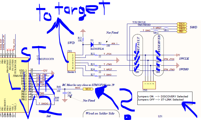
Posted on April 17, 2013 at 01:31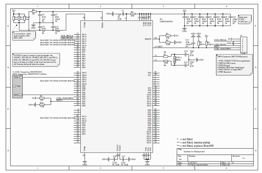 KLICK above image Any suggestions for improvements ??? 2. Could you again have a look at my JTAG connection? I need to use the STM32F4Discovery ST-Link2 with 6pin connector. Did I wire up my F405 correctly? Did I forget anything? What is it about that MCO pin (see picture of STM32F4Discovery ST-Link2 schematic). This one is connected on the STM32F4Discovery board but not via the SWD-connector. What is it? Do I need it? *confusion*. As far as I could get it the MCO is connected to PH0 (Oscillator in). What why and why not on SWD-connector?
 3. Reading through the STM32F4Discovery manual I found a note I don't get:
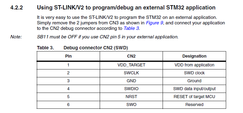 Why does it say I need to remove SB11 in order to use the CN2 (SWD-Connector) NRST pin? What happens if I don't remove SB11? I just don't get it. 4. Could you again have a look at my minimal schmematic pdf file. This time it's all about the bootloader. I intend to use the CAN-Bootloader (CAN2). Is that wiring correct? In AN2606 (general bootloader) it says: ''The hardware required to put the STM32F40xxx/41xxx into System memory boot mode consists of any circuitry, switch or jumper, capable of holding the BOOT0 pin high and the BOOT1 pin low during reset.''. Having a look at the STM32F4Discovery schematics I can see both BOOT0 and BOOT1 connected via a voltage divider between VDD(3V3) and GND with 10K and 510R.
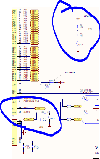 But god WHY WHY WHY? By the way SB18 and SB19 are fitted. Any explanations? Thank you very much and sorry for my confusing schematic. I'm just getting into it. Thanks for your patience and for reading. Greetings from Germany Michael
Hi,
currently I am trying to analyze the STM32F4Discovery schematic to get a minimal circuit using a STM32F407 oder STM32F405 in LQFP100. So I started an now ended up completely confused with a whole bunch of questions in my head: 1. Could anyone have a look at my minimal circuit? >>>>>>>>>>>>>>>>>>>>>>>http://www.uploadarea.de/files/pekgj4xyk4c9yujy1m6oawxqz.pdf
<<<<<<<<<<<<<<<<<<<<<<<<<< KLICK above image Any suggestions for improvements ??? 2. Could you again have a look at my JTAG connection? I need to use the STM32F4Discovery ST-Link2 with 6pin connector. Did I wire up my F405 correctly? Did I forget anything? What is it about that MCO pin (see picture of STM32F4Discovery ST-Link2 schematic). This one is connected on the STM32F4Discovery board but not via the SWD-connector. What is it? Do I need it? *confusion*. As far as I could get it the MCO is connected to PH0 (Oscillator in). What why and why not on SWD-connector?
 3. Reading through the STM32F4Discovery manual I found a note I don't get:
 Why does it say I need to remove SB11 in order to use the CN2 (SWD-Connector) NRST pin? What happens if I don't remove SB11? I just don't get it. 4. Could you again have a look at my minimal schmematic pdf file. This time it's all about the bootloader. I intend to use the CAN-Bootloader (CAN2). Is that wiring correct? In AN2606 (general bootloader) it says: ''The hardware required to put the STM32F40xxx/41xxx into System memory boot mode consists of any circuitry, switch or jumper, capable of holding the BOOT0 pin high and the BOOT1 pin low during reset.''. Having a look at the STM32F4Discovery schematics I can see both BOOT0 and BOOT1 connected via a voltage divider between VDD(3V3) and GND with 10K and 510R.
 But god WHY WHY WHY? By the way SB18 and SB19 are fitted. Any explanations? Thank you very much and sorry for my confusing schematic. I'm just getting into it. Thanks for your patience and for reading. Greetings from Germany Michael
2 REPLIES 2
Options
- Mark as New
- Bookmark
- Subscribe
- Mute
- Subscribe to RSS Feed
- Permalink
- Email to a Friend
- Report Inappropriate Content
2013-04-16 05:14 PM
Posted on April 17, 2013 at 02:14
I personally would do a single 10K for each on the BOOTx pins, with jumpers to VCC or GND. The arrangement ST has allows you to short with tweezers.
The MCO pin has often been used by DISCOVERY designs to provide 8 MHz to the primary CPU by using the 8 MHz from the ST-LINK CPU, which needs a crystal for USB. This would eliminate one 8 MHz crystal from the DISCOVERY BOM. A crystal based clock is desired for USB or CAN. NRST is bidirectional, assume you don't want the other processor driving it. Would perhaps add support for the LSE crystal on PC14/15, needed if you want to try STANDBY and RTC functionality. Honestly not hot about ST's evolving SWD header, would personally go for a classic 20-pin JTAG, or 10-pin SWD. Go with what even works for you, add options for multiple different header placements.
Tips, Buy me a coffee, or three.. PayPal Venmo
Up vote any posts that you find helpful, it shows what's working..
Up vote any posts that you find helpful, it shows what's working..
Options
- Mark as New
- Bookmark
- Subscribe
- Mute
- Subscribe to RSS Feed
- Permalink
- Email to a Friend
- Report Inappropriate Content
2013-04-17 12:27 AM
Posted on April 17, 2013 at 09:27
So for my conclusion:
1. BOOTx pins: 10k (btw. can you explain to me why the really make use of a voltage divider? For each BOOTpin both resistors + SB are placed.) 2. MCO pin: forget it. not important for me 3. thanks for the RTC hint 4. In other words I need to remove the SB connecting the DiscoveryNRST-pin to the DiscoveryST-Link in order to use the ST-Link for external programming??? 5. Unfortunately I dont have enough space for a 20pin JTAG. I'd like to use the 6pin although I in general don't like connectors which are not protected for reverse polarity. 6. Did you have a look at my JTAG connection? I don't want to order some PCB and not get a connection to the STM32F4. Thanks for you help. Short and precise. Excellent. Thanks.
Related Content
- OpenBootLoader Advice / Best Practice in STM32 MCUs Embedded software
- Some Bootloader questions in STM32 MCUs Products
- STM32H563: CubeProgrammer UART connect fails in PRODUCT_STATE = iROTProvisioned in STM32 MCUs Security
- STM32H747I-DISCO Jump To DFU BootLoader in STM32 MCUs Boards and hardware tools
- STM32C071 bootloader patterns and boot selector bits defaults in STM32 MCUs Embedded software