- STMicroelectronics Community
- STM32 MCUs
- STM32 MCUs Products
- STM32F103 ADC supply config
- Subscribe to RSS Feed
- Mark Topic as New
- Mark Topic as Read
- Float this Topic for Current User
- Bookmark
- Subscribe
- Mute
- Printer Friendly Page
STM32F103 ADC supply config
- Mark as New
- Bookmark
- Subscribe
- Mute
- Subscribe to RSS Feed
- Permalink
- Email to a Friend
- Report Inappropriate Content
2018-04-15 1:06 AM
Hi to all
datasheet
13587 Rev 17
5.3.1 table 9 says:
Vdda must be same potential as Vdd with a maximum diff of 300mV (footnote).
5.3.18 table 46 says: Vdda must be between 2.4 - 3.6 and not mentioning anything about Vdd
and
AN2834
2.2.12 says: it is desirable to have separate analog and digital supplies.so the question is: how can i manage Vdda - Vdd <= 300mV with different
supplies during opration and especially during power up?
and 2 other question about Vref,
AN2834 suggests using linear regulators but usually they have errors in different temperatures,do you suggest using reference voltage ICs?
also about using a separate 3.3v voltage reference ic for Vref: in table 46 of datasheet max rate for Vref is mentioned Vdda, and using different 3.3 supplies doesn't guaranty exact same 3.3000 voltage for both Vref and VDDa, is this difference going to be a problem or can i forget about it?
my supply is: SMPS DCtoDC 12-5 and in next level two separate LDOreg 5-3.3 for Vdda and Vdd.
#adc-configuration- Labels:
-
ADC
- Mark as New
- Bookmark
- Subscribe
- Mute
- Subscribe to RSS Feed
- Permalink
- Email to a Friend
- Report Inappropriate Content
2018-04-18 4:58 AM
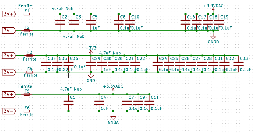
I use this circuit to remove the noisy parts from the processor.
I use SMC diodes to dissipate 1.2V headroom reducing the heat in the 3v3 reg by 60%
These PNP type regulators will work down to 200mV headroom and supply up to 1A
Otherwise you can use the same Regulator and Ferrites to isolate the noise.

- STM32H755ZI custom board not detected by ST-Link in STM32 MCUs Products
- STM32F103TBU6 Bare Die / Wafer Availability for R&D Prototyping in STM32 MCUs Products
- STM32H753XIH6 port K alternate functions TIM1 and TIM8 not working in STM32 MCUs Products
- Nucleo-H753ZI SPI Slave DMA continuously outputs 0xFF 0xFF 0xFF 0xFF; cannot transmit data in STM32 MCUs Embedded software
- Custom External Loader won't work until BOOT0 is pulled HIGH in STM32 MCUs Embedded software
