- STMicroelectronics Community
- STM32 MCUs
- STM32 MCUs Products
- Re: Regarding GPIO Feature
- Subscribe to RSS Feed
- Mark Topic as New
- Mark Topic as Read
- Float this Topic for Current User
- Bookmark
- Subscribe
- Mute
- Printer Friendly Page
Regarding GPIO Feature
- Mark as New
- Bookmark
- Subscribe
- Mute
- Subscribe to RSS Feed
- Permalink
- Email to a Friend
- Report Inappropriate Content
2014-11-23 05:05 AM
Hi, Ive been using several MCU before. Its my first time to use STMicro.
Now Im currently studying its architecture.My question is, what is the use of GPIO BSRR (Bit Set Reset Register) when we can access or write each bit with GPIO ODR (Output Data Register)?We can use Bitwise Or and Bitwise and to write each bit right?We can also bit banding for the same function right?I am curious if there is a special application where we can take advantage of this register.For now, i only see it as redundancy. Please help me understand the product.Thanks,Best Regards,Michael Javier #stm32-gpio-architecture- Labels:
-
GPIO-EXTI
- Mark as New
- Bookmark
- Subscribe
- Mute
- Subscribe to RSS Feed
- Permalink
- Email to a Friend
- Report Inappropriate Content
2014-11-23 06:08 AM
On the ARM architecture Loading and Storing aren't particularly rapid, doing a RMW* operation will take at least three instructions, four if the address needs loading. Peripheral registers are ''volatile'' so must be read each time they are used, the compiler can't cache them in processor registers.
Peripheral registers are not like regular memory. You can write the GPIO latches directly via ODR. If you want to set specific bits high or low, and don't know the current state of them, using BSRR allows you to set and reset multiple bits, in a single atomic write which modifies the GPIO latches in one action. A write to BSRR is like a RMW on ODR, done at a hardware level. *RMW - Read Modify Write ODR &= ~1; ODR |= 2; ODR ^= 5; Bit banding isn't particularly effective either, and has hazards on the TIMUp vote any posts that you find helpful, it shows what's working..
- Mark as New
- Bookmark
- Subscribe
- Mute
- Subscribe to RSS Feed
- Permalink
- Email to a Friend
- Report Inappropriate Content
2015-08-14 05:58 PM
- Mark as New
- Bookmark
- Subscribe
- Mute
- Subscribe to RSS Feed
- Permalink
- Email to a Friend
- Report Inappropriate Content
2015-08-14 06:18 PM
If it's a problem with other code loaded on the board you can strap BOOT(0) pin to VDD, then reset, try to connect and erase like that.
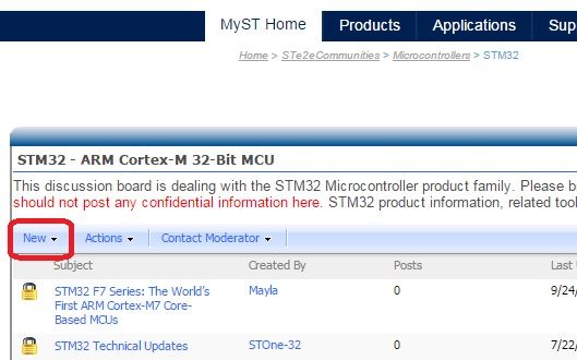
Alternately you can see if you have a ''Connect Under Reset'' option, either in IAR, or through the ST-LINK Utilities.Starting new threads, click ''New'' in top left immediately above the list of posts.Up vote any posts that you find helpful, it shows what's working..
- Mark as New
- Bookmark
- Subscribe
- Mute
- Subscribe to RSS Feed
- Permalink
- Email to a Friend
- Report Inappropriate Content
2015-08-14 06:22 PM
Up vote any posts that you find helpful, it shows what's working..
- Mark as New
- Bookmark
- Subscribe
- Mute
- Subscribe to RSS Feed
- Permalink
- Email to a Friend
- Report Inappropriate Content
2015-08-15 11:33 PM
Thanks for the fast support.
I tried the option 2 first and, that is to use the option connect during reset, but another error output as follow:Sun Aug 16, 2015 14:07:40: Loaded macro file: C:\Program Files (x86)\IAR Systems\Embedded Workbench 6.5\arm\config\flashloader\ST\FlashSTM32F4xxx.mac Sun Aug 16, 2015 14:07:40: Selecting SWD as current target interface. Sun Aug 16, 2015 14:07:40: Hardware reset with strategy 2 was performed Sun Aug 16, 2015 14:07:40: Initial reset was performed Sun Aug 16, 2015 14:07:41: 736 bytes downloaded and verified (3.84 Kbytes/sec) Sun Aug 16, 2015 14:07:41: Warning: Verify error, failed to read memory at address 0x20000000 - 0x2000001F Sun Aug 16, 2015 14:07:41: Warning: Verify error at address 0x20000000, target byte: 0x16, byte in file: 0x00 Sun Aug 16, 2015 14:07:41: Warning: Verify error at address 0x20000002, target byte: 0x00, byte in file: 0x02 Sun Aug 16, 2015 14:07:41: Warning: Verify error at address 0x20000003, target byte: 0x00, byte in file: 0x20 Sun Aug 16, 2015 14:07:41: Warning: Verify error at address 0x20000004, target byte: 0x16, byte in file: 0x05 ... and so on ...Sun Aug 16, 2015 14:07:41: Warning: Too many verify errors, only the first 200 are displayed Sun Aug 16, 2015 14:07:57: Fatal error: There were warnings during download of FLASH loader, see Log Window Session aborted! Sun Aug 16, 2015 14:07:57: Failed to load flash loader: C:\Program Files (x86)\IAR Systems\Embedded Workbench 6.5\arm\config\flashloader\ST\FlashSTM32F4xxx.out Sun Aug 16, 2015 14:07:57: Failed to load flash loader: C:\Program Files (x86)\IAR Systems\Embedded Workbench 6.5\arm\config\flashloader\ST\FlashSTM32F4xxx.flash For the first method, my undeerstunding is I have to desolder SB18 so that BOOT0 will be pull up instead of pulldown. I havent yet tried this, I will try it tomorrow when I get to the lab. Thanks.Best Regards,Michael Javier- Mark as New
- Bookmark
- Subscribe
- Mute
- Subscribe to RSS Feed
- Permalink
- Email to a Friend
- Report Inappropriate Content
2015-08-17 07:39 PM
Hi Clive,
I already tried the option 1 that is to connect boot 0 to VDD, and it woks!Thank you very much.- STM32U5G7VJT6Q GPIO Input issue in STM32 MCUs Boards and hardware tools
- Touchgfx with usb host CDC VCP in STM32 MCUs TouchGFX and GUI
- STM32CubeIDE project for BLE 5.4 PAwR feature on NUCLEO-WB09KE in STM32 MCUs Wireless
- STM32G0B1 USB Host not working in STM32 MCUs Products
- STM32F407G-DISC1 "Error reading value" in debug mode in STM32 MCUs Boards and hardware tools
