- STMicroelectronics Community
- STM32 MCUs
- STM32 MCUs Products
- Problem while writing to SPI data register on Nucl...
- Subscribe to RSS Feed
- Mark Topic as New
- Mark Topic as Read
- Float this Topic for Current User
- Bookmark
- Subscribe
- Mute
- Printer Friendly Page
Problem while writing to SPI data register on Nucleo-64 , STM32F411-re
- Mark as New
- Bookmark
- Subscribe
- Mute
- Subscribe to RSS Feed
- Permalink
- Email to a Friend
- Report Inappropriate Content
2020-02-05 5:13 AM
I am new to this nucleo board ( Nucleo-64 , STM32F411-re). I've configured SPI1 port as master and SPI4 port as slave. I am trying to establish communication between these two ports and verifying the data weather its reflecting on SPI1-> DR data registers.
I am having some doubts
- Is it possible to establish communication between two SPI ports on same board( SPI1 and SPI4 )
- Do this board has any loopback register so that I can verify the data I am sending
- Am I configured SPI registers correctly?? for above mentioned task
- Am I configured SPI NSS pin correctly??, provide I am configuring in Software mode as mentioned in the usermanual.
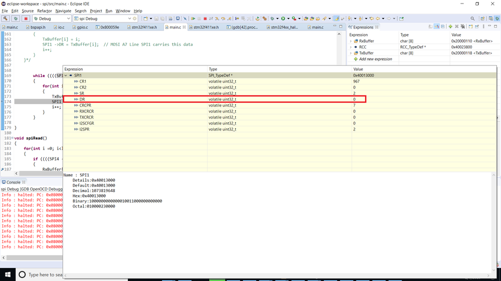
While debugging and watching the value of SPI-> DR register I am not able to see any values in the SPI Data register
// ----------------------------------------------------------------------------

#include <stdio.h>
#include <stdlib.h>
#include "diag/Trace.h"
#include "stm32f4xx.h"
#include "stm32f4xx_hal_gpio.h"
#include "stm32f4xx_hal.h"
// ----------------------------------------------------------------------------
//
// Standalone STM32F4 empty sample (trace via DEBUG).
//
// Trace support is enabled by adding the TRACE macro definition.
// By default the trace messages are forwarded to the DEBUG output,
// but can be rerouted to any device or completely suppressed, by
// changing the definitions required in system/src/diag/trace_impl.c
// (currently OS_USE_TRACE_ITM, OS_USE_TRACE_SEMIHOSTING_DEBUG/_STDOUT).
//

// ----- main() ---------------------------------------------------------------

// Sample pragmas to cope with warnings. Please note the related line at
// the end of this function, used to pop the compiler diagnostics status.
#pragma GCC diagnostic push
#pragma GCC diagnostic ignored "-Wunused-parameter"
#pragma GCC diagnostic ignored "-Wmissing-declarations"
#pragma GCC diagnostic ignored "-Wreturn-type"
#define size 8

char TxBuffer[size];
char RxBuffer[size];
char length = 8;

void init_periperalclock()   //init_peripheralClock();
{
	  /* Enable GPIO clock */
	  RCC->AHB1ENR |= (RCC_AHB1ENR_GPIOAEN | RCC_AHB1ENR_GPIOBEN);   //Port A clock enable

	  /* Enable SPI clock */
	  RCC->APB2ENR |= (RCC_APB2ENR_SPI1EN|RCC_APB2ENR_SPI4EN);  //SPI 1 Clock enable
	  //RCC->APB1ENR |= 16384;   //SPI 2 Clock enable
}
void init_gpio()
{

	/* Connections are as follows
	 * PA4 --> PB12  Slave select
	 * PA5 --> PB13  SCLK
	 * PA6 --> PA11  MISO
	 * PA7 --> PA1   MOSI
	 */

	// SPI1 --> PA4 - SS, PA5 - SCLK, PA6 - MISO, PA7 - MOSI
	GPIOA ->MODER |= (GPIO_MODER_MODER4_0|GPIO_MODER_MODER5_1|GPIO_MODER_MODER6_1|GPIO_MODER_MODER7_1); // PA5 PA6 PA7 - AF & PA4 - SS  // 256 + 2048 + 8192 + 32678 == 43264
	GPIOA ->OSPEEDR |= (GPIO_OSPEEDER_OSPEEDR4|GPIO_OSPEEDER_OSPEEDR5|GPIO_OSPEEDER_OSPEEDR6|GPIO_OSPEEDER_OSPEEDR7); // High speed
	GPIOA ->OTYPER |= (GPIO_ODR_ODR_4|GPIO_ODR_ODR_5|GPIO_ODR_ODR_6|GPIO_ODR_ODR_7); //Open drain
	GPIOA ->PUPDR |= (GPIO_PUPDR_PUPDR4_0|GPIO_PUPDR_PUPDR5_0|GPIO_PUPDR_PUPDR6_0|GPIO_PUPDR_PUPDR7_0);  // Push pull
    //GPIOA ->AFR[0] = 0x0050;

    // SPI4 --> PB12 - SS, PB13 - SCLK, PA1 - MOSI, PA11 - MISO
	GPIOA ->MODER |= (GPIO_MODER_MODER1_1|GPIO_MODER_MODER11_1);
	GPIOB ->MODER |= ((GPIO_MODER_MODER12_0|~GPIO_MODER_MODER12_0)|GPIO_MODER_MODER13_1);

	GPIOA ->OSPEEDR |=(GPIO_OSPEEDER_OSPEEDR1|GPIO_OSPEEDER_OSPEEDR11);
	GPIOB ->OSPEEDR |= (GPIO_OSPEEDER_OSPEEDR12|GPIO_OSPEEDER_OSPEEDR13); // High speed

	GPIOA ->OTYPER |= (GPIO_ODR_ODR_1|GPIO_ODR_ODR_11);
	GPIOB->OTYPER |= (GPIO_ODR_ODR_12|GPIO_ODR_ODR_13); // Open drain

	GPIOA ->PUPDR |= (GPIO_PUPDR_PUPDR1_0|GPIO_PUPDR_PUPDR11_0);
	GPIOB ->PUPDR|= (GPIO_PUPDR_PUPDR12_0|GPIO_PUPDR_PUPDR13_0);  // Push pull

	// PA5 - SCLK for SPI1, PA6 - MISO for SPI1, PA7 - MOSI for SPI1
	GPIOA ->AFR[0] = ((5<<20)|(5<<24)|(5<<28));
	GPIOA ->AFR[0] = 5<<4;  // PA1 - MOSI for SPI4
	GPIOA ->AFR[1] = 6<<12; // PA11- MISO for SPI4
	GPIOB ->AFR[1] = 6<<20; // PB13- SCLK for SPI4
}

void init_spiParameters()
{
	/* Setting up parameters for SPI1 (Master)
	  This configuration corresponds to MOSI
	  as Output Data and MISO as Input data*/
	SPI1 ->SR |= 0;
	SPI1 ->CR1 |= (SPI_CR1_BR_1 & ~SPI_CR1_BR_1); // Baud rate is set to fper/2
	SPI1 ->CR1 |= (SPI_CR1_CPOL|SPI_CR1_CPHA); // Setting up clock polarity and phase
 	SPI1 ->CR1 |= (SPI_CR1_DFF & ~SPI_CR1_DFF); // Selecting 8 bit data format // After this line BSY flag is setting
	SPI1 ->CR1 |= SPI_CR1_LSBFIRST; // Selecting LSB value first for transmission
	SPI1 ->CR1 |= (SPI_CR1_SSM | SPI_CR1_SSI); // Slave select Output Enable
	SPI1 ->CR1 |= (SPI_CR1_MSTR | SPI_CR1_SPE);  // Declaring SPI1 as Master


	/* Setting up parameters for SPI4 (Slave)
	  This configuration corresponds to MISO
	  as Output Data and MOSI as Input data*/
	SPI4 ->CR1 |= (SPI_CR1_DFF & ~SPI_CR1_DFF);  // setting up DFF bit
	SPI4 ->CR1 |= (SPI_CR1_CPOL|SPI_CR1_CPHA); // Setting up clock polarity and phase
	SPI4 ->CR1 |= SPI_CR1_LSBFIRST; // Selecting LSB value first for transmission
	SPI4 ->CR1 |= SPI_CR1_SSM;  // Enabling SSM bit
	SPI4 ->CR1 |= (SPI_CR1_SSI & ~SPI_CR1_SSI); //Resetting SSI bit
	SPI4 ->CR1 |= SPI_CR1_SPE;  // Enabling SPI
	SPI4 ->CR1 |= (SPI_CR1_MSTR & ~SPI_CR1_MSTR); // Declaring SPI4 as Slave
}

void spiWrite()
{
	for(int i=0; i<length;)
	{
		if ((((SPI1 ->SR) & SPI_SR_TXE) == SPI_SR_TXE))
		{
			TxBuffer[i] = i;
			SPI1 ->DR = TxBuffer[i];  // MOSI A7 Line SPI1 carries this data
			i++;
		}
	}

}

void spiRead()
{
	for(int i =0; i<length;)
	{
		if ((((SPI4 ->SR) & SPI_SR_RXNE) == SPI_SR_RXNE))
		{
			RxBuffer[i] = SPI4 ->DR;  // MISO Line of SPI4 receives data
			i++;
	    }
	}

}

int
main(int argc, char* argv[])
{

  init_periperalclock();
  init_gpio();
  init_spiParameters();
  spiWrite();
  spiRead();

}

#pragma GCC diagnostic pop

// ----------------------------------------------------------------------------
- Labels:
-
SPI
-
STM32F4 Series
- Mark as New
- Bookmark
- Subscribe
- Mute
- Subscribe to RSS Feed
- Permalink
- Email to a Friend
- Report Inappropriate Content
2020-02-05 5:50 AM
Didn't look at all register setup details, just one remark: you have to poll in an endless loop for SPI_SR_TXE and SPI_SR_RXNE
conditions. Therefore, you need another while loop within the for.
> Is it possible to establish communication between two SPI ports on same board( SPI1 and SPI4 )
Yes, thats possible. But I doubt that it will work with a sequential spiWrite() and spiRead() because write and read occur on the same SPI clock cycles. For short messages the FIFOs might help, but in general people use interrupt or DMA features for simultaneous write+read.
- Mark as New
- Bookmark
- Subscribe
- Mute
- Subscribe to RSS Feed
- Permalink
- Email to a Friend
- Report Inappropriate Content
2020-02-07 12:22 AM

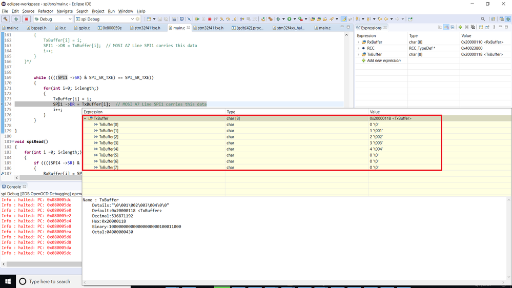
I've edited code as you've mentioned above, Still I couldn't find an changes also the data isn't reflected/ written to SPI Data register. I have attached screenshots for your reference. If subsequent read and write is a problem, I had change the code such that It performs only spiWrite(), still the data is not written into the register.
while ((((SPI1 ->SR) & SPI_SR_TXE) == SPI_SR_TXE))
		{
			for(int i=0; i<length;)
			{
				TxBuffer[i] = i;
				SPI1 ->DR = TxBuffer[i];  // MOSI A7 Line SPI1 carries this data
				i++;
			}
}- Mark as New
- Bookmark
- Subscribe
- Mute
- Subscribe to RSS Feed
- Permalink
- Email to a Friend
- Report Inappropriate Content
2020-02-07 1:43 AM
> Therefore, you need another while loop within the for.
You have to wait (poll) for each and every individual byte/char.
Here is a small example using SPI2 and SPI3 on a Nucleo-F446RE. It assumes that the GPIOs are already configured and copies the string from tx to rx buffer via SPI:
static char tx[16] = "Hello\r\n";
  static char rx[16];

  SPI2->CR1 = 0;
  SPI2->CR1 |= SPI_CR1_SSM;			// NSS in software
  SPI2->CR1 |= SPI_CR1_SSI;			// Internal slave select
  SPI2->CR1 |= SPI_CR1_MSTR;			// master mode
  SPI2->CR1 |= 5 << SPI_CR1_BR_Pos;		// 64:1 bitrate
  SPI2->CR1 |= SPI_CR1_SPE;			// SPI enable

  SPI3->CR1 = 0;
  SPI3->CR1 |= SPI_CR1_SSM;			// NSS in software
  SPI3->CR1 |= SPI_CR1_SPE;			// SPI enable

  for( int i=0; i<strlen(tx); ++i )
  {
	  while( !(SPI2->SR & SPI_SR_TXE) ); // poll for TX empty
	  SPI2->DR = tx[i];

	  while( !(SPI3->SR & SPI_SR_RXNE) ); // poll for RX non-empty
	  rx[i] = SPI3->DR;
  }

HAL_UART_Transmit( &huart2, rx, strlen(rx), HAL_MAX_DELAY );
Note that this is a toy example because the slave SPI needs to poll all the time to listen for (and not to miss) incoming chars. So, finally you might want to add interrupt handling or DMA. Note also that slave select is not handled here.
- STM32F401CCU6 I2C3 + DMA TX works electrically, DMA TC fires, but AW9523 never receives data in STM32 MCUs Embedded software
- STM32F411RE (Nucleo) PWM TIM1_CH1 - PA8 appears shorted to 5V when powered, unaffected by BOOT0 or NRST. in STM32 MCUs Boards and hardware tools
- GPDMA & HPDMA on STM32N6 in STM32 MCUs Products
- Clarification Needed on SYSCFG Register Map for STM32F411RE in STM32 MCUs Embedded software
- No I2C communication with Nucleo-F411RE and ADXL345 in STM32 MCUs Boards and hardware tools
