- STMicroelectronics Community
- STM32 MCUs
- STM32 MCUs Products
- Re: Noise levels in ADC in STM32L4?
- Subscribe to RSS Feed
- Mark Topic as New
- Mark Topic as Read
- Float this Topic for Current User
- Bookmark
- Subscribe
- Mute
- Printer Friendly Page
Noise levels in ADC in STM32L4?
- Mark as New
- Bookmark
- Subscribe
- Mute
- Subscribe to RSS Feed
- Permalink
- Email to a Friend
- Report Inappropriate Content
2017-09-19 2:41 PM
I have a custom board using an STM32L452. I'm doing some testing of the ADC and am finding pretty high levels of noise.
I have a rail-to-rail op amp driving the ADC pin with a 300 ohm resistor from the amp to the pin and a .047uF cap to ground at the pin. The board is laid out well, with lots of ground under and around the chip, and bypass caps on every power pin, right next to the pins. Plus a bulk 10uF ceramic on the Vdd. The Vaa has it's own .1uF and 10uF right next to the pin. The Vdd and the Vaa each have a ferrite separating them from the main board power source (and therefore from each other).
In addition, to try and reduce external noise during my tests I added several extra caps on top of the cap on the ADC pin. A .1uF, a 1uF, and a 10uF ceramic, all stacked on top of the original cap. I did the same series on top of the bypass cap for the Vaa. (these extra caps will be removed after the tests) Those caps are all X7R and progressively larger physical packages to overcome the DC Bias issue ceramic caps have.
The input signal is a constant DC biased in the middle of the input range.
In the DMA interrupt routine I look at each result from that one channel and compare it to a previously stored high and low value. If the new one is higher than the old high, it replaces it. If lower than the old low value, it replaces it. After 100,000 conversions I save that high and low value in another pair of variables and reset the pair used in the comparison. Those saved values are then read via I2C by an external device that displays them and the difference between them. So that LCD shows me the high and low value for the past 100,000 conversions plus the difference between them.
In an ideal ADC that difference would be zero. In my previous version of this board (same op amp driving the ADC) I had a PIC24 chip, and with 12 bit conversions (and no additional caps) I saw typical conversions that fluctuated by about 4-6 numbers. With this board and its STM32L452 I am seeing typical variations in the range of about 13 to 22 numbers. About 4 times more noise than the PIC.
I tried various settings for the ADC clock prescaler, both synchronous and asynchronous, divided by 1, 2, and 4. And tried all the different sampling times. There were small changes at different settings, but not a large amount. The results ranged from 13-16 numbers different up to 19-22 numbers different. So varying from about 3.5 to 4.5 bits worth of noise instead of the 2 to 2.5 bits worth of noise I had with the PIC.
That means that at 12 bit conversions I'm really only seeing 7 to 8 bits of clean signal.
I tried the oversampling, and it does help. But I need conversions at a decent rate and it would take 256 times oversampling to recover about 4 bits. That would reduce the speed far too much for my application. This is going to process control voltages in the audio frequency range, not extremely slow sensors, where I could get by with excessive filtering in both the hardware and software.
Has anybody else done an extensive test of the ADC on an L4 (or other STM32)? And are you seeing similar amounts of noise in the raw conversions?
- Mark as New
- Bookmark
- Subscribe
- Mute
- Subscribe to RSS Feed
- Permalink
- Email to a Friend
- Report Inappropriate Content
2017-09-19 8:49 PM
Have you tried testing on a STM32L452RE Nucleo64 board? Testing on a reference design would eliminate potential external issues in your board design.
I have run into issues sourcing VDD and VDDA from the same power plane. The LDO I had driving VDD had a fairly poor step response to load (the power supply was optimized for minimum quiescent current in standby) and the load steps were apparent on VDD and VDDA even with the recommended filtering in place. A 10mA voltage change on VREF was enough to lose 3.5 bits.
The solution in my case was to use a separate low noise LDO for VDDA that could be shut down in standby.
Test against a reference design with nothing else going on and see if you still see the same amount of noise.
- Mark as New
- Bookmark
- Subscribe
- Mute
- Subscribe to RSS Feed
- Permalink
- Email to a Friend
- Report Inappropriate Content
2017-09-20 12:12 PM
Thanks for the reply. I don't have a Nucleo board available to test with. That's why I'm asking about other peoples experiences with this.
Your experience, and the 3.5 bit reduction in noise is useful information. But it's not clear if you still had noticeable noise after that reduction, before doing any software filtering. If you were converting at full speed, and after adding the fix that gained you 3.5 bits, did you still have 4 bits or so of noise in the raw unfiltered, un-oversampled data? Or was it much lower?
If you and others are using an L4 and are seeing much less than 4 bits of noise when converting at full speed, and looking at the raw conversion data (no oversampling or software filtering), then it's worth my time to rip apart the hardware and try to reduce noise on the Vaa and ADC input. But if everybody is seeing that level of noise, then it's a internal problem and doesn't require me reworking the board.
- Mark as New
- Bookmark
- Subscribe
- Mute
- Subscribe to RSS Feed
- Permalink
- Email to a Friend
- Report Inappropriate Content
2017-09-22 2:36 PM
So nobody else has done basic testing to see how much noise they are getting in the ADC when running at full speed, without added oversampling or software filtering?
- Mark as New
- Bookmark
- Subscribe
- Mute
- Subscribe to RSS Feed
- Permalink
- Email to a Friend
- Report Inappropriate Content
2017-09-22 4:17 PM
One of the nastiest problem I ever debugged was similar to yours. The hardware was Nucleo L476RG based with the application hardware on a proper designed (ground planes + decoupling + short signal lines + buffer amps, input impedance around 100 kΩ !) extension board. That way I eliminated �?just as Riggs stated�? problems with the MCU layout. During measurement, I stopped the MCU (to save power and noise) and let the DMA do the job. Upon completion I transmitted the data via UART to a PC for evaluation and started the next cycle. According to the theory the RMS noise due to discretion of a perfect A/D is 1/√ 12 (approx 0.29 digits). The measured RMS noise was between 0.36 … 0.42 digits. This met the noise level (10.5 … 10.9 bits resolution) as specified in table 65 of
http://www.st.com/resource/en/datasheet/stm32l476je.pdf
. But after I had replaced the HAL API by the LL API, the first half of the buffer was noisy (RMS noise about 1 digit equivalent to raising the noise power by a factor of 6) while the second half was fine (around 0.4 digits). “No problem,� I said to myself and enlarged the buffer. This let the noisy part grow as well as the clean part. Inserting a sleep before the next cycle fixed the problem.The solution of the puzzle was: Replacing the HAL API by LL I raised the Baud rate. LL was way faster. Doing so, the RS232/USB chip (good ole PL2303 TA) required more power. For high baud rates (1 MBaud) and big buffers (32 KBytes) the voltage converter in the PL2303TA was still running when the next conversion had started already. The interface chip was “in the cable� between the MCU board and the PC. What can we make of it?
- If set up properly (hardware and software) the STM32L4 has a low noise A/D converter.
- Even off-board components can mess up A/D conversion.
- Mark as New
- Bookmark
- Subscribe
- Mute
- Subscribe to RSS Feed
- Permalink
- Email to a Friend
- Report Inappropriate Content
2017-09-23 12:13 AM
I had a very similar problem with the STM32F407 MCU. It was the trickiest thing I ever debug. The ADC noise was dependent of the code position in the flash memory - adding some NOPs significantly changed the ADC noise. The problem appeared to be inside the MCU. Code position had influence on the flash memory prefetch operation. The solution was to disable ART Flash Prefetcher (bit FLASH_ACR_PRFTEN should be cleared in the FLASH->ACR register). You can try it with you L4 MCU, it may help.
- Mark as New
- Bookmark
- Subscribe
- Mute
- Subscribe to RSS Feed
- Permalink
- Email to a Friend
- Report Inappropriate Content
2017-09-23 2:04 AM
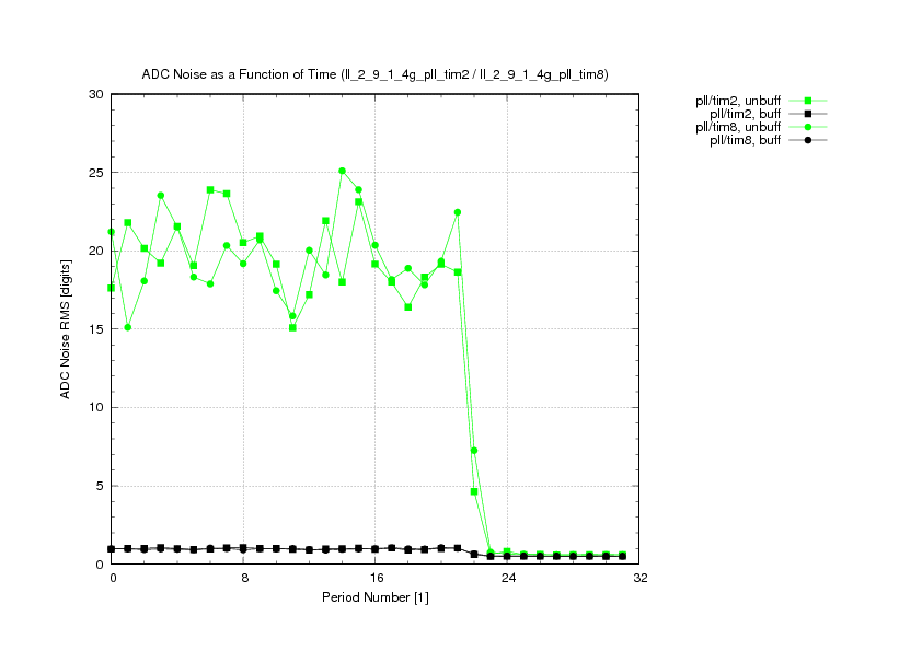
A picture is worth a thousand words. Four pictures are even better. To give you an idea of what you should possibly consider if you are facing A/D noise I browsed my old records.

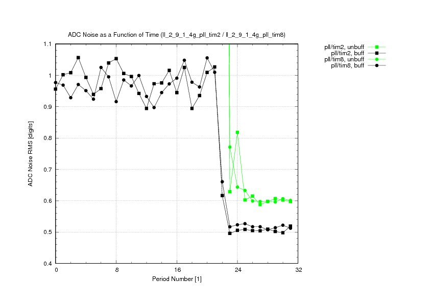
This is, where I started. The PL2303TA was bustling about up to period 22 to recover from the 1 MBaud / 32 KByte transmission of the most recent cycle. The RMS noise of the unbuffered (green) system went up to about 20 digits. Keep in mind that the noise of the perfect system is ? 0.29. Buffering (using the internal OpAmp) helped a lot. To investigate the data in the idle period of the PL2303TA, I zoomed the y-scale:

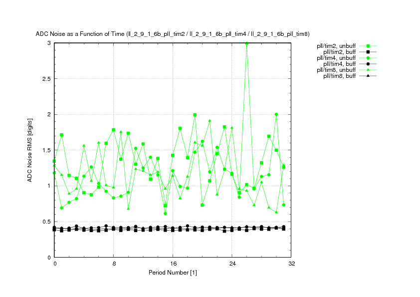
Same graph as above, just enlarged. After taming the interface (reducing the transmission speed to 19200 Baud), things look much better:

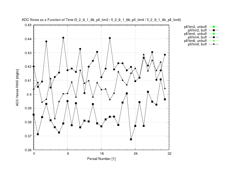
Now the buffered systems approach the theoretical limit of 0.29. Though the CPU was stopped, I required the timers for triggering the ADC. I tried TIM2, TIM4, and TIM8. The following is a zoomed plot for the buffered systems:

The graph suggests that the noise could depend on the timer. But to prove that, more measurements would be required. My application used TIM2.
Bottom line:
- Whenever you use the ADCs, evaluate.
- The data sheet tells you what you can expect if you are doing a good job.
- There are more parameters that I expected. I?d never thought the timers could be a factor too.
- I tried to use SysTick for triggering. For that I had to keep up the CPU running. The results were so bad that I even did not record them ?.
- Noise depends on the sampling time (and the input impedance). In my system the S/N did not improve for sampling times beyond 12.5 cycles.
- Mark as New
- Bookmark
- Subscribe
- Mute
- Subscribe to RSS Feed
- Permalink
- Email to a Friend
- Report Inappropriate Content
2017-09-23 2:13 PM
Since two of the suggestions pointed to issues with the voltage regulation, I decided to tack on a separate precision LDO on the Vaa. It's a regulator with 0.1% load regulation and is soldered literally on top of the bypass cap for the Vdda/Vssa, about 1mm away from the chip pins.
No difference.
Not entirely surprising, since the main 3.3v regulator is a larger LDO that also has 0.1% load regulation. But it now rules out the regulator.
- Mark as New
- Bookmark
- Subscribe
- Mute
- Subscribe to RSS Feed
- Permalink
- Email to a Friend
- Report Inappropriate Content
2017-09-23 2:52 PM
In order to eliminate noise on the input pin and op-amp as being the issue, I disconnected the pin from the op-amp and simply connected it to a 200 ohm to ground and a 200 ohm to Vaa, with the same stack of ceramic caps (0.047uF, 0.1uF, 1uF, and 10uF) to ground. All very close to the chip. So that's a 100 ohm source impedance. (less, when you count the impedance of the caps)
It made no difference.
So with the Vaa ruled out, and the input signal ruled out, I'm down to it being internal interference inside the MCU.
- Mark as New
- Bookmark
- Subscribe
- Mute
- Subscribe to RSS Feed
- Permalink
- Email to a Friend
- Report Inappropriate Content
2017-09-23 3:07 PM
Hello Dave.
Take a look also to
Has a lot of usefull info, SW and HW methods to improve accuracy and noise figure.
Regards
vf
- Ambient noise level is not updating when in Detect mode in STM32 MCUs Products
- Where is ADF ambient noise level stored for SAD? in STM32 MCUs Embedded software
- STM32F105VCT micro GPIO input thresholds in STM32 MCUs Products
- Countermeasure of hardware noise for software interrupt GPIO-EXTI line in STM32 MCUs Products
- IBIS model STM32F765 no output in STM32 MCUs Products