- STMicroelectronics Community
- STM32 MCUs
- STM32 MCUs Products
- Re: How does memory work in Cortex M3?
- Subscribe to RSS Feed
- Mark Topic as New
- Mark Topic as Read
- Float this Topic for Current User
- Bookmark
- Subscribe
- Mute
- Printer Friendly Page
How does memory work in Cortex M3?
- Mark as New
- Bookmark
- Subscribe
- Mute
- Subscribe to RSS Feed
- Permalink
- Email to a Friend
- Report Inappropriate Content
2017-10-18 07:21 AM
Hi,
Now I'm trying to understand about how do the memories work.
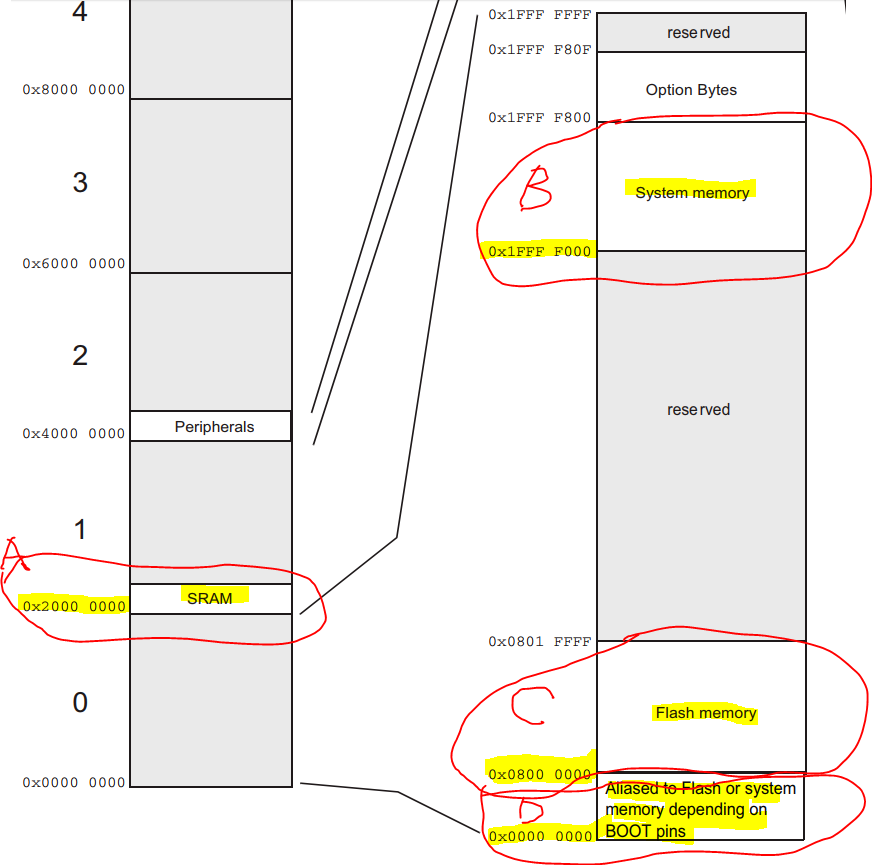
I've attached STM32F103C8's memory map and I've highlighted each memory in the image (aka A, B, C, D)..
In here, I want to know what exactly relationship between B(System memory) and C(Flash memory)?
and What is the D(aliased to Flash or system Memory area)? Is D real existing physically?
If I use JTAG to upload the compiled hex file into the Cortex Flash memory, then where exactly does it go ? A?B?C?D?
after complete upload the firmware code, then what happens? D just copy from C?

I think B, C and D is supposed to be as
#memory-map- Mark as New
- Bookmark
- Subscribe
- Mute
- Subscribe to RSS Feed
- Permalink
- Email to a Friend
- Report Inappropriate Content
2017-10-18 07:45 AM
They are all decoded from high order address bits, look perhaps at some classic microprocessor texts where a 74138 logic chip takes in the high order bits and decodes discrete memory regions.
The FLASH memory is at 0x080XXXXX within the memory map, this is where you write your binary image of the firmware to be run.
The there is the SHADOWING concept, where a memory may appear in TWO, or more, places within the memory map. When the BOOT pins select FLASH, then it appears at BOTH 0x08000000 and 0x00000000. This is important because the processor boots assuming the vector table is starting at zero, ie SCB->VTOR = 0
Up vote any posts that you find helpful, it shows what's working..
- Mark as New
- Bookmark
- Subscribe
- Mute
- Subscribe to RSS Feed
- Permalink
- Email to a Friend
- Report Inappropriate Content
2017-10-18 09:21 AM
It might be interesting to read up on C start up code and examining the parts of your linker script that it interacts with (there's probably plenty you probably don't care about in there) as well. Understanding the code that runs before calling your main() can really connect the dots with the memories.
- Mark as New
- Bookmark
- Subscribe
- Mute
- Subscribe to RSS Feed
- Permalink
- Email to a Friend
- Report Inappropriate Content
2017-10-18 09:47 AM
Up vote any posts that you find helpful, it shows what's working..
- Mark as New
- Bookmark
- Subscribe
- Mute
- Subscribe to RSS Feed
- Permalink
- Email to a Friend
- Report Inappropriate Content
2017-10-18 10:00 AM
Thanks for letting me know,
'
When the BOOT pins select FLASH, then it appears at BOTH 0x08000000 and 0x00000000.'
Did you mean that when the boot pins selected FLASH, then
0x08000000
is alliased to 0x00000000?
In other word, If I modify 0x00000004 adddress data, then 0x08000004 also be modified? and vice versa?
- Mark as New
- Bookmark
- Subscribe
- Mute
- Subscribe to RSS Feed
- Permalink
- Email to a Friend
- Report Inappropriate Content
2017-10-18 10:10 AM
Alias or Shadow, choose the word you prefer. I would write into the 0x08000000 space, but the 0x00000000 space would probably work for that purpose too. There would be less dependency on internal settings if you work with the memory location that will always be present.
You should be able to read the same 32-bit word for 0x00000004 or 0x08000004, look in your debugger memory viewer or ST-LINK Utilities some time. This typically points back into an address in the 0x080XXXXXX range, and thus control is transferred to the natural address of the memory in question.
Up vote any posts that you find helpful, it shows what's working..
- Mark as New
- Bookmark
- Subscribe
- Mute
- Subscribe to RSS Feed
- Permalink
- Email to a Friend
- Report Inappropriate Content
2017-10-18 12:28 PM
Honestly I think some 40 year old books on Computer Architecture and Microprocessor Interfacing might be significantly more illuminating in this case in terms of understanding how the parts come together. Today's SoC solutions just pull all the basic concepts into a chip level solution, the memory decoding and busing remain inherently the same. People used to have college level classes on this stuff.
Up vote any posts that you find helpful, it shows what's working..
- OPENAMP STM32H745 memory problems in STM32 MCUs Embedded software
- Nucleo H755ZI-Q lwip in STM32 MCUs Embedded software
- adding code to a project without CubeMX deleting it in STM32CubeMX (MCUs)
- Throughput on STM32H533 OCTOSPI external Flash + Ram in STM32 MCUs Embedded software
- Best solution to control an ILI9341 TFT LCD in STM32 MCUs Products