- STMicroelectronics Community
- STM32 MCUs
- STM32 MCUs Products
- Driving 5V bus transceiver with 5V tolerant pins
- Subscribe to RSS Feed
- Mark Topic as New
- Mark Topic as Read
- Float this Topic for Current User
- Bookmark
- Subscribe
- Mute
- Printer Friendly Page
Driving 5V bus transceiver with 5V tolerant pins
- Mark as New
- Bookmark
- Subscribe
- Mute
- Subscribe to RSS Feed
- Permalink
- Email to a Friend
- Report Inappropriate Content
2020-06-12 10:56 AM
Good evening (o;
I know that most GPIO pins can be driven from 5V devices...
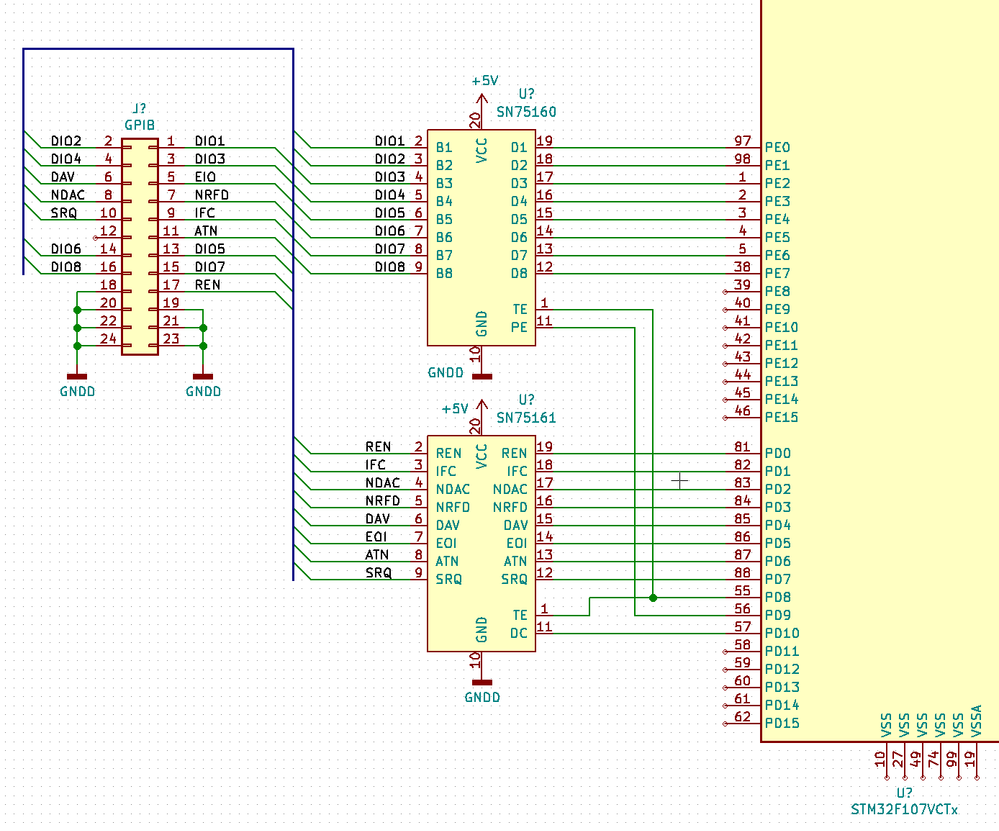
But how about connecting a 5V bus transceiver? Is that also save?
Or better to use a level shifter in between?
Reason for asking: Project involving SN75160/161 bus transceivers for GPIB interface....
thanks in advance
richard
- Labels:
-
GPIO-EXTI
- Mark as New
- Bookmark
- Subscribe
- Mute
- Subscribe to RSS Feed
- Permalink
- Email to a Friend
- Report Inappropriate Content
2020-06-12 5:23 PM
Old school TTL uses 0.8V low and 2.4V high input logic levels.
It should work without level shifters.
For more detailed answer, just post exact schematic.
- Mark as New
- Bookmark
- Subscribe
- Mute
- Subscribe to RSS Feed
- Permalink
- Email to a Friend
- Report Inappropriate Content
2020-06-13 2:01 AM
Good morning (o;
No full schematic yet..but a simplified version with the chosen MCU STM32F107VCT..
- Mark as New
- Bookmark
- Subscribe
- Mute
- Subscribe to RSS Feed
- Permalink
- Email to a Friend
- Report Inappropriate Content
2020-06-18 2:13 AM
Seems to work that way..though only tested so far in one direction...
At least I see commands and data coming from the GPIB bus on the Nucleo-F207 USB console (o;
CMD: 40 	MTA0
CMD: 3F 	UNLISTEN
CMD: 25 	MLA5
DAT: *
DAT: I
DAT: D
DAT: N
DAT: ?
CMD: 3F 	UNLISTEN
CMD: 20 	MLA0
CMD: 45 	MTA5
Now I only have to find an easy and elegant way how to switch certain GPIO pins from output to input...
Or can I always read the GPIO input when it is configured as GPIO open drain output with pull up?
- Mark as New
- Bookmark
- Subscribe
- Mute
- Subscribe to RSS Feed
- Permalink
- Email to a Friend
- Report Inappropriate Content
2020-06-18 1:58 PM
AN4899 Application note
STM32 GPIO configuration for hardware settings and low-power consumption
Page 17:
However, a GPIO is five-volt tolerant only in input mode.
When the output mode is enabled, the GPIO is no more five-volt tolerant.
For more details about I/O input voltage, refer to VIN
parameters in the general operating conditions table of the datasheet.
DocID029601 Rev 1
==============================
The above guide suggests that a IO output connected to TTL output (high level) could create over-voltage problem.
A simple fix is to use Bidirectional Voltage-Level Shifter with Auto Direction Sensing
- Mark as New
- Bookmark
- Subscribe
- Mute
- Subscribe to RSS Feed
- Permalink
- Email to a Friend
- Report Inappropriate Content
2020-06-18 2:04 PM
Hmmm...so far I didn't had problems with it...though I used data bus only in receiving mode...
but the GPIB control bus is mixed....so I could read GPIB control signals as well as driving control signals....otherwise the above GPIB bus capture wouldn't have be possible...
The SN75161 device is not a straight transceiver from left to right or vice versa....
so for example I tested DAV being read from MCU and NRFD/NDAC being driven by MCU....so far the MCU survived it (o;
Guess special care must be taken at which time the GPIO direction configuration and the transceiver direction change takes place...
- STM32G431 Bootloader issue in STM32 MCUs Products
- Tip: A super-simple circuit for auto-detecting hardware variants in Others: STM32 MCUs related
- VBUS Sensing enable - USB FS STM32H7A3 - Nucleo Board in STM32 MCUs Boards and hardware tools
- STM32F769I-DISCO Using CAN interface over Arduino connector in STM32 MCUs Products
