- STMicroelectronics Community
- STM32 MCUs
- STM32 MCUs Products
- Delay with Center Aligned PWM triggering an ADC co...
- Subscribe to RSS Feed
- Mark Topic as New
- Mark Topic as Read
- Float this Topic for Current User
- Bookmark
- Subscribe
- Mute
- Printer Friendly Page
Delay with Center Aligned PWM triggering an ADC conversion
- Mark as New
- Bookmark
- Subscribe
- Mute
- Subscribe to RSS Feed
- Permalink
- Email to a Friend
- Report Inappropriate Content
2016-08-01 7:28 AM
Hi,
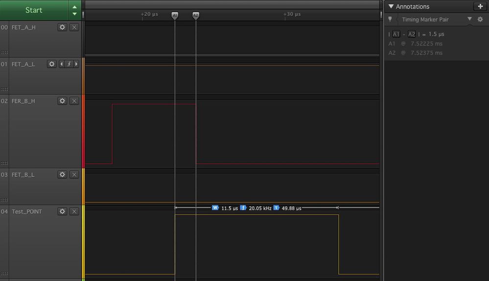
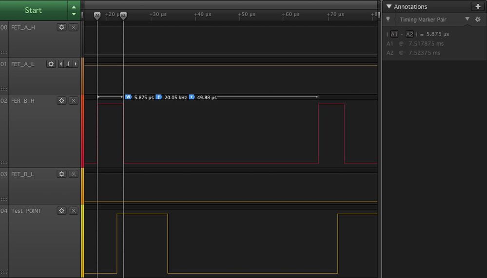
I’m using a stm32f103 to generate center aligned PWM on which i have synced a dual regular simultaneous injected mode ADC conversion.I’m using TIM4 as source of the PWM signal and, to launch the ADC acquisition at the center of the signal i’m using the update event checking the direction of the counter (this way i have one acquisition every two update events - i cannot use TIM1 and the related repetition counter).As you can see from the posted image, the whole ADC acquisition takes 11.5us and starts about 1.4us after the center of the PWM pulse and this is a little trouble. The crucial data to be acquired, are located at the start of the acquisition, first two channels, so 2.2us from the start of the acquisition.- FET_B_H (red): center aligned pwm signal- Test_POINT(yellow): set high in the TIM4 ISR routine (along with the ADC SOC) and set back low at the end of the conversion (by the DMA TC1 ISR).I cannot explain the constant delay of 1.4us between the update event and jump to the ISR code that triggers the ADC conversion. Maybe someone of you can help me to figure this out. Attached you can see the init code for both the ADC and TIM4.Thank you,Davide
- Mark as New
- Bookmark
- Subscribe
- Mute
- Subscribe to RSS Feed
- Permalink
- Email to a Friend
- Report Inappropriate Content
2016-08-01 7:36 AM
The Init code for the DMA and ADC:
void
adcInit(void
) {
ADC_InitTypeDef
ADC_InitStructure;
DMA_InitTypeDef
DMA_InitStructure;
NVIC_InitTypeDef
NVIC_InitStructure; // DMA InitDMA_DeInit(DMA1_Channel1);
DMA_InitStructure.
DMA_PeripheralBaseAddr
= (uint32_t)ADC1 + 0x4c;DMA_InitStructure.
DMA_MemoryBaseAddr
= (uint32_t)&adcRawData[0];DMA_InitStructure.
DMA_DIR
= DMA_DIR_PeripheralSRC;DMA_InitStructure.
DMA_BufferSize
= (uint32_t)9;DMA_InitStructure.
DMA_PeripheralInc
= DMA_PeripheralInc_Disable;DMA_InitStructure.
DMA_MemoryInc
= DMA_MemoryInc_Enable;DMA_InitStructure.
DMA_PeripheralDataSize
= DMA_PeripheralDataSize_Word;DMA_InitStructure.
DMA_MemoryDataSize
= DMA_MemoryDataSize_Word;DMA_InitStructure.
DMA_Mode
= DMA_Mode_Circular;DMA_InitStructure.
DMA_Priority
= DMA_Priority_VeryHigh;DMA_InitStructure.
DMA_M2M
= DMA_M2M_Disable;DMA_Init(DMA1_Channel1, &DMA_InitStructure);
DMA_ITConfig(DMA1_Channel1, DMA_IT_TC,
ENABLE
);DMA_ClearITPendingBit(DMA1_IT_GL1 | DMA1_IT_TC1 | DMA1_IT_HT1);
DMA_Cmd(DMA1_Channel1,
ENABLE
);// Enable the DMA1_Channel1 global Interrupt
NVIC_InitStructure.
NVIC_IRQChannel=
DMA1_Channel1_IRQn;
NVIC_InitStructure.
NVIC_IRQChannelPreemptionPriority= 0;
NVIC_InitStructure.
NVIC_IRQChannelSubPriority
= 0;NVIC_InitStructure.
NVIC_IRQChannelCmd
=ENABLE
;NVIC_Init(&NVIC_InitStructure);
// ADC1 configuration
ADC_InitStructure.
ADC_Mode
= ADC_Mode_RegInjecSimult;ADC_InitStructure.
ADC_ScanConvMode
=ENABLE
;ADC_InitStructure.
ADC_ContinuousConvMode=
DISABLE;
ADC_InitStructure.
ADC_ExternalTrigConv
= ADC_ExternalTrigConv_None;ADC_InitStructure.
ADC_DataAlign
= ADC_DataAlign_Right;ADC_InitStructure.
ADC_NbrOfChannel
= 9;ADC_Init(ADC1, &ADC_InitStructure);
ADC_RegularChannelConfig(ADC1, ADC_Channel_5, 1, ADC_SAMPLE_TIME);
ADC_RegularChannelConfig(ADC1, ADC_Channel_10, 2, ADC_SAMPLE_TIME);
ADC_RegularChannelConfig(ADC1, ADC_Channel_1, 3, ADC_SAMPLE_TIME);
ADC_RegularChannelConfig(ADC1, ADC_Channel_1, 4, ADC_SAMPLE_TIME);
ADC_RegularChannelConfig(ADC1, ADC_Channel_3, 5, ADC_SAMPLE_TIME);
ADC_RegularChannelConfig(ADC1, ADC_Channel_3, 6, ADC_SAMPLE_TIME);
ADC_RegularChannelConfig(ADC1, ADC_Channel_12, 7, ADC_SAMPLE_TIME);
ADC_RegularChannelConfig(ADC1, ADC_Channel_13, 8, ADC_SAMPLE_TIME);
ADC_DMACmd(ADC1,
ENABLE
);// ADC2 configuration
ADC_InitStructure.
ADC_Mode
= ADC_Mode_RegInjecSimult;ADC_InitStructure.
ADC_ScanConvMode
=ENABLE
;ADC_InitStructure.
ADC_ContinuousConvMode=
DISABLE;
ADC_InitStructure.
ADC_ExternalTrigConv
= ADC_ExternalTrigConv_None;ADC_InitStructure.
ADC_DataAlign
= ADC_DataAlign_Right;ADC_InitStructure.
ADC_NbrOfChannel
= 9;ADC_Init(ADC2, &ADC_InitStructure);
ADC_RegularChannelConfig(ADC2, ADC_Channel_6, 1, ADC_SAMPLE_TIME);
ADC_RegularChannelConfig(ADC2, ADC_Channel_11, 2, ADC_SAMPLE_TIME);
ADC_RegularChannelConfig(ADC2, ADC_Channel_2, 3, ADC_SAMPLE_TIME);
ADC_RegularChannelConfig(ADC2, ADC_Channel_2, 4, ADC_SAMPLE_TIME);
ADC_RegularChannelConfig(ADC2, ADC_Channel_4, 5, ADC_SAMPLE_TIME);
ADC_RegularChannelConfig(ADC2, ADC_Channel_4, 6, ADC_SAMPLE_TIME);
ADC_RegularChannelConfig(ADC2, ADC_Channel_14, 7, ADC_SAMPLE_TIME);
ADC_RegularChannelConfig(ADC2, ADC_Channel_15, 8, ADC_SAMPLE_TIME);
ADC_ExternalTrigConvCmd(ADC2,
ENABLE
);// enable and calibrate
ADC_Cmd(ADC1,
ENABLE
);adcCalibrateADC(ADC1);
ADC_Cmd(ADC2,
ENABLE
);adcCalibrateADC(ADC2);
// setup injection sequence
ADC_InjectedSequencerLengthConfig(ADC1, 1);
ADC_InjectedSequencerLengthConfig(ADC2, 1);
ADC_InjectedChannelConfig(ADC1, ADC_Channel_5, 1, ADC_SAMPLE_TIME);
ADC_InjectedChannelConfig(ADC2, ADC_Channel_4, 1, ADC_SAMPLE_TIME);
ADC_ExternalTrigInjectedConvCmd(ADC1,
ENABLE
);ADC_ExternalTrigInjectedConvCmd(ADC2,
ENABLE
);ADC_ExternalTrigInjectedConvConfig(ADC1, ADC_ExternalTrigInjecConv_None);
ADC_ExternalTrigInjectedConvConfig(ADC2, ADC_ExternalTrigInjecConv_None);
// Start ADC1 / ADC2 Conversions for first time
ADC_ExternalTrigConvCmd(ADC1,
ENABLE
);ADC_SoftwareStartConvCmd(ADC2,
ENABLE
);}
- Mark as New
- Bookmark
- Subscribe
- Mute
- Subscribe to RSS Feed
- Permalink
- Email to a Friend
- Report Inappropriate Content
2016-08-01 7:47 AM
The init code for TIM4
void
fetSetBaseTime(int32_t period) {
TIM_TimeBaseInitTypeDef
TIM_TimeBaseStructure;
NVIC_InitTypeDef
NVIC_InitStructure;NVIC_InitStructure.
NVIC_IRQChannel
= SYNC_TIMER_IRQn;NVIC_InitStructure.
NVIC_IRQChannelPreemptionPriority= 0;
NVIC_InitStructure.
NVIC_IRQChannelSubPriority= 0;
NVIC_InitStructure.
NVIC_IRQChannelCmd
=ENABLE
;NVIC_Init(&NVIC_InitStructure);
// TIM Init FET_H_TIMER == TIM4
TIM_TimeBaseStructInit(&TIM_TimeBaseStructure);
TIM_TimeBaseStructure.
TIM_Prescaler
= 1;// 36Mhz
TIM_TimeBaseStructure.
TIM_Period
= period-1;TIM_TimeBaseStructure.
TIM_CounterMode
= TIM_CounterMode_CenterAligned1;TIM_TimeBaseInit(FET_H_TIMER, &TIM_TimeBaseStructure);
TIM_ClearITPendingBit(FET_H_TIMER, TIM_IT_Update);
TIM_ITConfig(FET_H_TIMER, TIM_IT_Update,
ENABLE
); //OC INITFET_H_TIMER_REMAP;
TIM_OCStructInit(&TIM_OCInitStructure);
TIM_OCInitStructure.
TIM_OCMode
= TIM_OCMode_PWM1;TIM_OCInitStructure.
TIM_OutputState
= TIM_OutputState_Enable;TIM_OCInitStructure.
TIM_Pulse
= fetDutyCycle;TIM_OCInitStructure.
TIM_OCPolarity
= TIM_OCPolarity_High;// Phase A
TIM_OC1Init(FET_H_TIMER, &TIM_OCInitStructure);
TIM_OC1PreloadConfig(FET_H_TIMER, TIM_OCPreload_Enable);
// Phase B
TIM_OC2Init(FET_H_TIMER, &TIM_OCInitStructure);
TIM_OC2PreloadConfig(FET_H_TIMER, TIM_OCPreload_Enable);
// Phase C
TIM_OC3Init(FET_H_TIMER, &TIM_OCInitStructure);
TIM_OC3PreloadConfig(FET_H_TIMER, TIM_OCPreload_Enable);
TIM_ARRPreloadConfig(FET_H_TIMER,
ENABLE
);TIM_Cmd(FET_H_TIMER,
ENABLE
);}
void
FET_H_TIMER_IRQHandler(void
){if
(TIM_GetITStatus(FET_H_TIMER, TIM_IT_Update) !=RESET
) {TIM_ClearITPendingBit(FET_H_TIMER, TIM_IT_Update);
//Check the DIR bit of CR1 TIM3 register for
upcounting
.
if
((FET_H_TIMER->CR1
& 0x0010) == 0){digitalHi(tp); // SET THE TP HIGH AT THE START OF THE CONVERSION
ADC_SoftwareStartConvCmd(ADC1,
ENABLE
);}
}
}
- Mark as New
- Bookmark
- Subscribe
- Mute
- Subscribe to RSS Feed
- Permalink
- Email to a Friend
- Report Inappropriate Content
2016-08-01 9:56 AM
If there is the need of additional information or measurement feel free to ask, i will provide them as soon as possibile!
The firmware is intended to run a small three phase inverter for BLDC motor control.Thank you again,Davide- STM32 MCU with 5V Logic I/O and PWM-Synchronized ADC Trigger? in STM32 MCUs Products
- STM32U585 need help with getting ADC -> DMA working in trivial case. in STM32 MCUs Products
- How to Toggle a Debug Pin When ADC Conversion Starts in DMA Mode on STM32? in STM32 MCUs Products
- STM32H503 SVD / RM ADC_CFGR_EXTSEL logical error? in STM32 MCUs Embedded software
- STM32H743 SPI DMA delay in STM32 MCUs Embedded software
