- STMicroelectronics Community
- STM32 MCUs
- STM32 MCUs Boards and hardware tools
- STM32F411RE PCB Layout
- Subscribe to RSS Feed
- Mark Topic as New
- Mark Topic as Read
- Float this Topic for Current User
- Bookmark
- Subscribe
- Mute
- Printer Friendly Page
STM32F411RE PCB Layout
- Mark as New
- Bookmark
- Subscribe
- Mute
- Subscribe to RSS Feed
- Permalink
- Email to a Friend
- Report Inappropriate Content
2020-11-17 4:00 AM
Hi there,
i finished my program and the schematic design of my prototype. Now i want to start with the PCB layout. Therefore i have some questions regarding the Supply & Oscillators. At the beginning i implemented the DFU for programming the STM32F4, because of that i added a 8 MHz OSC on the Pins PH1-OSC_IN & PH1-OSC_Out. But actually i want to be able to debug my program so i included an JTAG/SWD Pinheader.
If i am using an ST-Link/V2 programmer to load my programm into the chip, do i still need this Oscillator?
I use the internal PLL clock to generate an 40 kHz signal using Timer Callbacks. Do i still need the 32kHz OSC on the Pins PC14-PSC_IN & PC15-OSC_OUT like on the NUCLEO Board?
Where should i place the Capacitors on the Supply Voltage, right next to the VDD Pins?
The Buttons i implemented are on NRST/BOOT0 and on two GPIO outputs. Do i actually need to Boot Button because now im using JTAG/SWD instead of DFU, where i need to start in Boot mode?
Did i use the right Pull Down resistors on the Buttons?
I would appreciate some tipps and tricks, i will add some pictures of the schematic.
regards
Walter
- Labels:
-
RCC
-
STM32F4 Series
- Mark as New
- Bookmark
- Subscribe
- Mute
- Subscribe to RSS Feed
- Permalink
- Email to a Friend
- Report Inappropriate Content
2020-11-17 4:59 AM
There is a useful app note: dm00115714-getting-started-with-stm32f4xxxx-mcu-hardware-development-stmicroelectronics.pdf.
You don't need the boot switch, only the pull-down if you only flash via SWD. Flashing via the internal boot loader is meant for updates in-the-field where the customer doesn't have a ST-LINK avail.
RESET switch depends on who is using the MCU. In the lab you can always do a cold start or reset via SWD. Reset is IO so you might think of using it as a board level reset (if applicable) or not using it at all.
hth
KnarfB
- Mark as New
- Bookmark
- Subscribe
- Mute
- Subscribe to RSS Feed
- Permalink
- Email to a Friend
- Report Inappropriate Content
2020-11-17 5:26 AM
To programm the chip you don't need an external oscillator (HSE) , because on reset the MCU uses an internal oscillator.
Humm... The 32K osc is not related to PLL.
If you don't have a HSE oscillator, you have to use the internal HSI oscillator to drive the PLL. Beware the HSI precision il low.
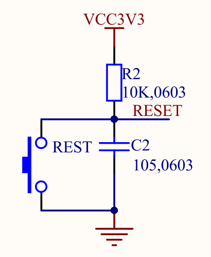
Your pulldown on reset/boot is useless because when the button is open, it is connected to nothing.
You can use something like this:

- Mark as New
- Bookmark
- Subscribe
- Mute
- Subscribe to RSS Feed
- Permalink
- Email to a Friend
- Report Inappropriate Content
2020-11-17 5:37 AM
> when the button is open, it is connected to nothing
wrong. There is an internal pull-up, see "Figure 4. Reset" circuit in der app note mentioned above.
- Mark as New
- Bookmark
- Subscribe
- Mute
- Subscribe to RSS Feed
- Permalink
- Email to a Friend
- Report Inappropriate Content
2020-11-17 5:47 AM
- Mark as New
- Bookmark
- Subscribe
- Mute
- Subscribe to RSS Feed
- Permalink
- Email to a Friend
- Report Inappropriate Content
2020-11-19 2:25 AM
"Where should i place the Capacitors on the Supply Voltage, right next to the VDD Pins?" Ideally surface mount bypass/decoupling capacitors should be placed as near to the micro as possible to minimise EMI, ADC noise etc.. The path back to ground should be as short as possible too. Assuming a two layer board, it is good practice to make the bottom layer a "ground plane" and minimise routing tracks on this layer. Think of the capacitors as tanks of electrons - the easier the micro can get at these electrons the less noise your micro will make. Small valued capacitors close to the micro are able to respond quickly to the switching demands of the micro, while larger valued caps further away respond less quickly but keep the smaller caps "topped up" with electrons... it's really not that dissimilar to plumbing - the goal is to keep the micro(pump) from running dry and making noise in the tracks(pipes)...
- BLE fails on cold boot, but works perfectly after entering FUS mode. in STM32 MCUs Wireless
- STM32WL RF Layout – Routing Signals on 3rd Layer Near RF Section & Stack-up Changes in STM32 MCUs Wireless
- Custom STM32h743ZI Board wont connect ("Failed to initialize DAP") in STM32 MCUs Boards and hardware tools
- Clarification on Secure Boot Flow with PCROP Protection for STM32H723 in STM32 MCUs Security
- RF Trace & Layout Review - STM32WL LoRa, 433MHz in STM32 MCUs Wireless