- STMicroelectronics Community
- STM32 MCUs
- STM32 MCUs Products
- Multiplexing SRAM,NOR Flash and NAND Flash ?
- Subscribe to RSS Feed
- Mark Topic as New
- Mark Topic as Read
- Float this Topic for Current User
- Bookmark
- Subscribe
- Mute
- Printer Friendly Page
Multiplexing SRAM,NOR Flash and NAND Flash ?
- Mark as New
- Bookmark
- Subscribe
- Mute
- Subscribe to RSS Feed
- Permalink
- Email to a Friend
- Report Inappropriate Content
2014-04-25 04:36 PM
Guys,
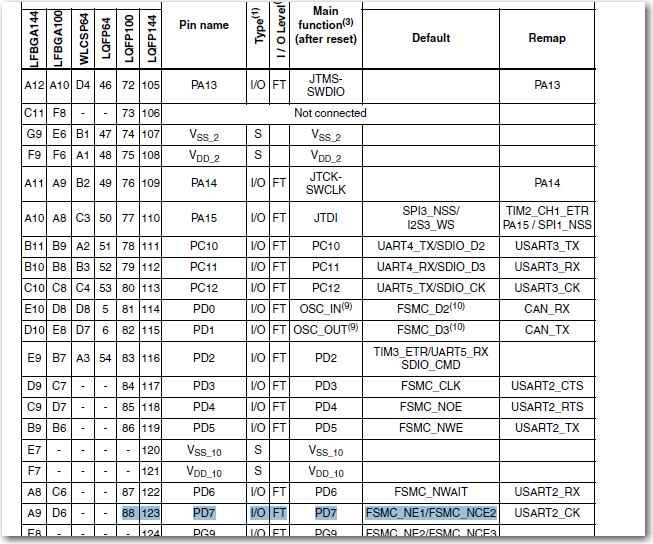
How can I multiplex SRAM,NOR Flash and NAND Flash on PD7 ? It's function as PD7 FSMC_NE1/FSMC_NCE2 on pin 88 for STM32F103VCT6, is it configurable via software or I need to put a latch / multiplex chip for it ? Any examples for it (schematic)? What's the common application for NAND flash ? Can I run my code from NOR Flash ? I saw there's boot option ''System memory is selected as boot space'', page 48 STM32 reference, chapter 2.4 Boot Configuration... Thanks #fsmc- Labels:
-
FMC-FSMC
- Mark as New
- Bookmark
- Subscribe
- Mute
- Subscribe to RSS Feed
- Permalink
- Email to a Friend
- Report Inappropriate Content
2014-04-25 04:57 PM
You'd probably want to gate it with a high order address bit.
System Memory is the OTP ROM at 0x1FFFFxxx, and which contains the system loader. You'd have to put some start up code in Flash to configure the external bus before you could execute-in-place off the NOR device, and this would run slower on the external bus.Up vote any posts that you find helpful, it shows what's working..
- Mark as New
- Bookmark
- Subscribe
- Mute
- Subscribe to RSS Feed
- Permalink
- Email to a Friend
- Report Inappropriate Content
2014-04-25 05:03 PM
Can I run the code from NAND flash ? I have NAND flash only now, how can I upload the code to NAND flash ?
thanks- Mark as New
- Bookmark
- Subscribe
- Mute
- Subscribe to RSS Feed
- Permalink
- Email to a Friend
- Report Inappropriate Content
2014-04-25 06:15 PM
NAND devices are block access, like a hard drive, you can't execute-in-place, you'd need to copy the data into RAM and you could run it from there.
You see NAND and Serial NOR devices on Embedded Linux boards, what they typically do is copy the executable image in to a large SDRAM/DDRx memory, and have ARM9/10 CPU's with caches and memory management units.Up vote any posts that you find helpful, it shows what's working..
- Mark as New
- Bookmark
- Subscribe
- Mute
- Subscribe to RSS Feed
- Permalink
- Email to a Friend
- Report Inappropriate Content
2014-04-25 07:59 PM
Do you have a reference / example for schematic on using NAND and NOR with SRAM for STM32F103VCT6 ? The one I saw on ST3210 Eval is for STM32F103ZET6...
Thanks- Mark as New
- Bookmark
- Subscribe
- Mute
- Subscribe to RSS Feed
- Permalink
- Email to a Friend
- Report Inappropriate Content
2014-04-25 08:03 PM
Does you part have the FSMC? If it does aren't the pins used materially identical?
Up vote any posts that you find helpful, it shows what's working..
- Mark as New
- Bookmark
- Subscribe
- Mute
- Subscribe to RSS Feed
- Permalink
- Email to a Friend
- Report Inappropriate Content
2014-04-25 08:10 PM
Get the data sheets and work through the pin lists.
http://www.keil.com/mcbstm32exl/mcbstm32e-base-board-schematics.pdf
Up vote any posts that you find helpful, it shows what's working..
- Mark as New
- Bookmark
- Subscribe
- Mute
- Subscribe to RSS Feed
- Permalink
- Email to a Friend
- Report Inappropriate Content
2014-04-25 08:47 PM
Ok thanks for the info,
if I have 512x16 SRAM, it means I have 1 Mbyte of SRAM ? so if I want to have 4 Mbyte I can use 512x16 SRAM, 4 pieces, correct me if I'm wrong, thank you- Mark as New
- Bookmark
- Subscribe
- Mute
- Subscribe to RSS Feed
- Permalink
- Email to a Friend
- Report Inappropriate Content
2014-04-25 09:00 PM
Yes, 1MB
For multiple devices you'd either want to add your own decoder on the high order addresses, or see if the CSx provided by the STM32 are usable. In the old days you'd use something like an 74LS138 Renesas has a 64Mbit (8MB) part R1WV6416R, there might be othersUp vote any posts that you find helpful, it shows what's working..
- Mark as New
- Bookmark
- Subscribe
- Mute
- Subscribe to RSS Feed
- Permalink
- Email to a Friend
- Report Inappropriate Content
2014-04-26 07:09 PM
Thanks for the info,
I saw on STM32F103VCT6 Pin 88, PD7, FSMC_NE1/FSMC_NCE2 and
and How can I call PSRAM,NOR flash and NAND flash ? Will I controll them by software ? How can I control the NE1 Chip Select for two devices SRAM and NOR flash ? any clues ?thanks
- STM32F405 wont flash - 3D printer board. in STM32 MCUs Boards and hardware tools
- Application image integrity on stm32h7 flash in STM32 MCUs Products
- STOP2_Mode prevents me from programming the MCU using J-Link and STM32 Cube programmer in STM32 MCUs Boards and hardware tools
- Store values in STM32G0 internal flash in STM32 MCUs Products
- Error at start of debugging while Flash write test in STM32 MCUs Products