- STMicroelectronics Community
- STM32 MPUs
- STM32 MPUs Products and hardware related
- The new ANA0 / ANA1 pins
- Subscribe to RSS Feed
- Mark Topic as New
- Mark Topic as Read
- Float this Topic for Current User
- Bookmark
- Subscribe
- Mute
- Printer Friendly Page
The new ANA0 / ANA1 pins
- Mark as New
- Bookmark
- Subscribe
- Mute
- Subscribe to RSS Feed
- Permalink
- Email to a Friend
- Report Inappropriate Content
2019-07-16 2:00 AM
Hi,
I'm currently figuring out about the new ANA0 / ANA1 pins.
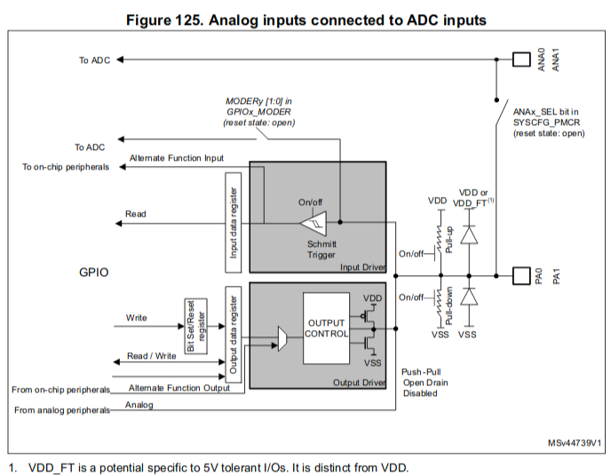
As far as I understand, those pins are always connected to the ADC so that I don't need to touch the GPIO registers in order to use those pins. Is my understanding correct?
Also I can connect those pin to PA0 / PA1 using ANAx_SEL bits in SYSCFG_PMCR register. In this case is it possible to short or damage the circuit/chip when I set different signal between ANAx and PAx?
Thanks a lot!
Solved! Go to Solution.
- Labels:
-
STM32MP15 Lines
Accepted Solutions
- Mark as New
- Bookmark
- Subscribe
- Mute
- Subscribe to RSS Feed
- Permalink
- Email to a Friend
- Report Inappropriate Content
2019-07-16 2:35 AM
Your understanding about ANA0/ANA1 is correct, they are always connected to ADC to avoid to go thru an analog switch (which is the case for all other ADC inputs, which due to its resistivity, could limit ADC sampling capacitor minimum charge time.
There is no need to any GPIO settings to use ANAx (obvious as not linked to a GPIO).
The ANAx_SEL are there for legacy usage, I did not see any rationale to use it in most cases (as there is as well other ADC inputs on PAx).
Yes, there is a small risk of damage, e.g. if you externally drive voltage on ANA0/ANA1 with low impedance and at same time driving PA0/PA1 in output or input while the 'switch' between ANAx/PAx is closed using ANAx_SEL.
Major concern of uncontrolled usage of IOs is current leakage in your system.
As a general rule, risk is there whenever the limit values in datasheet are not respected (i.e. injected current, input voltages, etc..). Otherwise, IOs are quite robusts and tolerant to most misuses.
So, to avoid issue, in case ANAx_SEL=1 is used, ANAx pin must be left open in the system.
- Mark as New
- Bookmark
- Subscribe
- Mute
- Subscribe to RSS Feed
- Permalink
- Email to a Friend
- Report Inappropriate Content
2019-07-16 2:12 AM
What chip are you talking about?
- Mark as New
- Bookmark
- Subscribe
- Mute
- Subscribe to RSS Feed
- Permalink
- Email to a Friend
- Report Inappropriate Content
2019-07-16 2:16 AM
I'm talking about STM32MP157x, and possibly all STM32 MPU series.
- Mark as New
- Bookmark
- Subscribe
- Mute
- Subscribe to RSS Feed
- Permalink
- Email to a Friend
- Report Inappropriate Content
2019-07-16 2:35 AM
Your understanding about ANA0/ANA1 is correct, they are always connected to ADC to avoid to go thru an analog switch (which is the case for all other ADC inputs, which due to its resistivity, could limit ADC sampling capacitor minimum charge time.
There is no need to any GPIO settings to use ANAx (obvious as not linked to a GPIO).
The ANAx_SEL are there for legacy usage, I did not see any rationale to use it in most cases (as there is as well other ADC inputs on PAx).
Yes, there is a small risk of damage, e.g. if you externally drive voltage on ANA0/ANA1 with low impedance and at same time driving PA0/PA1 in output or input while the 'switch' between ANAx/PAx is closed using ANAx_SEL.
Major concern of uncontrolled usage of IOs is current leakage in your system.
As a general rule, risk is there whenever the limit values in datasheet are not respected (i.e. injected current, input voltages, etc..). Otherwise, IOs are quite robusts and tolerant to most misuses.
So, to avoid issue, in case ANAx_SEL=1 is used, ANAx pin must be left open in the system.
- Mark as New
- Bookmark
- Subscribe
- Mute
- Subscribe to RSS Feed
- Permalink
- Email to a Friend
- Report Inappropriate Content
2019-07-16 4:41 AM
Well explained, thanks!
- STM32MP157 ADC failing to probe during boot in STM32 MPUs Products and hardware related
- STM32MP15x: How to enable / use ANA0, ANA01 analog pins in STM32 MPUs Products and hardware related
- ADC sampling from ANA0/ANA1 via M4 in STM32 MPUs Products and hardware related
- What is the correct Linux pin control configuration for ANA0 and ANA1 on TFBGA361? in STM32 MPUs Embedded software and solutions
- How can I use pin ANA0 and ANA1 as ADC. in STM32 MPUs Products and hardware related
