- STMicroelectronics Community
- STM32 MCUs
- STM32 MCUs Wireless
- Exposed pad in Stm32wb55rg connection with gnd man...
- Subscribe to RSS Feed
- Mark Topic as New
- Mark Topic as Read
- Float this Topic for Current User
- Bookmark
- Subscribe
- Mute
- Printer Friendly Page
Exposed pad in Stm32wb55rg connection with gnd mandatory or not?
- Mark as New
- Bookmark
- Subscribe
- Mute
- Subscribe to RSS Feed
- Permalink
- Email to a Friend
- Report Inappropriate Content
2024-02-29 10:55 AM - edited 2024-02-29 10:59 AM
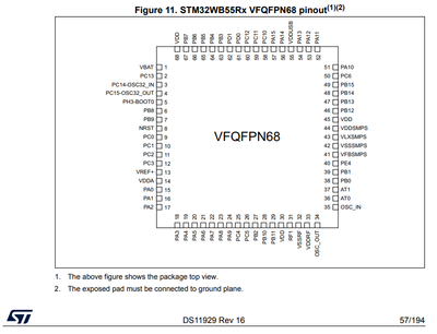
In my design I left the exposed pad in Stm32wb55rg VFQFN68 package. when I try to flash the device using st link , iam getting error "target not found". I am check the design and found i left the epad (69th pin) floating. Does this cause any issue ?. Please help me out here .thanks @Amel NASRI .
Solved! Go to Solution.
- Labels:
-
BLE
-
STM32WB series
Accepted Solutions
- Mark as New
- Bookmark
- Subscribe
- Mute
- Subscribe to RSS Feed
- Permalink
- Email to a Friend
- Report Inappropriate Content
2024-03-01 12:45 AM
Hello @ajaykrishna097 and welcome to the ST Community :smiling_face_with_smiling_eyes:.
So, as indicated on the DS11929, the exposed pad must be connected to ground plane:
So, for a working design, you need to connect the exposed pad to the GND plane.
Best Regards.
STTwo-32
To give better visibility on the answered topics, please click on Accept as Solution on the reply which solved your issue or answered your question.
- Mark as New
- Bookmark
- Subscribe
- Mute
- Subscribe to RSS Feed
- Permalink
- Email to a Friend
- Report Inappropriate Content
2024-03-01 2:21 AM
Just to reconfirm, if I didn't connect the exposed pad to gnd then my design "will not work". Sorry for asking it again , if this is a issue that will for cause the MCU to not work, then I will redesign and initiate the manufacturing.
- Mark as New
- Bookmark
- Subscribe
- Mute
- Subscribe to RSS Feed
- Permalink
- Email to a Friend
- Report Inappropriate Content
2024-03-01 2:23 AM
One more thing, I have drilled the pcb from the bottom of the MCU and reached the exposed pad and check the connectivity with gnd it is connected, is the exposed pad internally connected to VSS. Note: I have not connected the epad to gnd, I checked it in a non populated pcb the epad is just not connected to anything, after soldering the IC then there is a connectivity from epad and gnd may be it is internal connected
- Mark as New
- Bookmark
- Subscribe
- Mute
- Subscribe to RSS Feed
- Permalink
- Email to a Friend
- Report Inappropriate Content
2024-03-01 4:36 AM
To guarantee that the PCB will work on the best conditions, you should connect the exposed pad to the GND plane.
Best Regards.
STTwo-32
To give better visibility on the answered topics, please click on Accept as Solution on the reply which solved your issue or answered your question.
- STM32WB55RG: BLE software not working after upgrading BLE stack firmware in STM32 MCUs Wireless
- STM32WB55RG BLE not advertising when connected to 5V adaptor in STM32 MCUs Wireless
- STM32WB55 in STM32 MCUs Wireless
- failing to connect to the WB55 Nucleo using the STM32CubeMonitor-RF in STM32 MCUs Wireless
- VBUS Sensing on STM32N6 in STM32 MCUs Products
