- STMicroelectronics Community
- STM32 MCUs
- STM32 MCUs Products
- Re: Trouble communicating with a new board design ...
- Subscribe to RSS Feed
- Mark Topic as New
- Mark Topic as Read
- Float this Topic for Current User
- Bookmark
- Subscribe
- Mute
- Printer Friendly Page
Trouble communicating with a new board design - SWD ERROR
- Mark as New
- Bookmark
- Subscribe
- Mute
- Subscribe to RSS Feed
- Permalink
- Email to a Friend
- Report Inappropriate Content
2015-07-23 04:19 PM
This is my first project with an STM part. I have started development on a NUCLEO board with an STM32F401RE chip and I'm programming/debugging using the onboard STLINKv2. So far firmware development has gone well.
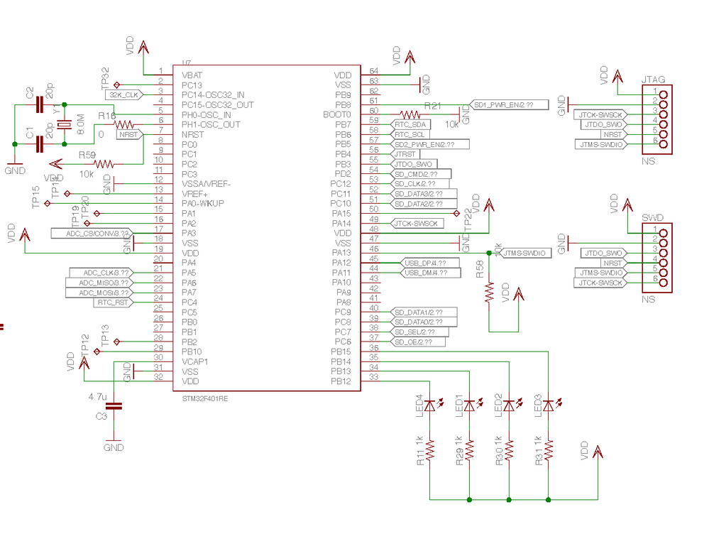
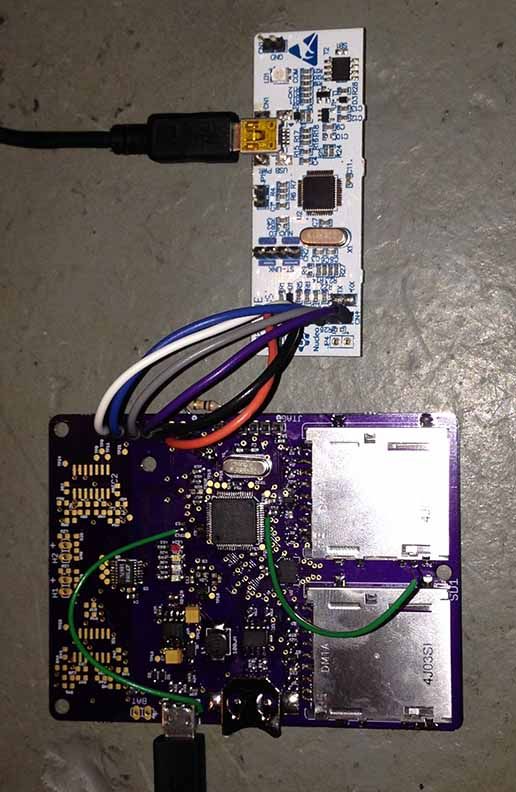
I designed a new board with the same chip (STM32F401RE) and I bought a second NUCLEO board to harvest the STLINK from. I cannot communicate with the new pcb at all -- from either STLINK, and I'm afraid I might have done something wrong in my schematic. I am attaching the schematic and a picture of my programming setup. Some notes: 1. I have removed the CN4 jumpers on the STLINK board2. I have tried with only SWDIO, SCK, GND, and VDD (also trying with SWO and NRST)3. I have tried various configurations of BOOT0, BOOT1, although by default BOOT0 = GND. 4. I have tested continuity all the way between the pins and the STLINK and made the wires shorter. No matter what I do, when I plug in the STLINK board, the NUCLEO drive contains a file called fail.txt, which contains the text ''SWD ERROR''. And I am unable to connect or communicate with the target board from the STLINK software.

- Mark as New
- Bookmark
- Subscribe
- Mute
- Subscribe to RSS Feed
- Permalink
- Email to a Friend
- Report Inappropriate Content
2015-07-23 05:19 PM
Can you attach a better focused/resolution picture, rather than in-line (100kb) one?
Check the voltage on the VCAP pin, and the NRST pin. Can you use the ST-LINK Utilities rather than the on-board mass-storage method? The board looks to have it's own supply, if so *don't* connect VDD to the ST-LINKUp vote any posts that you find helpful, it shows what's working..
- Mark as New
- Bookmark
- Subscribe
- Mute
- Subscribe to RSS Feed
- Permalink
- Email to a Friend
- Report Inappropriate Content
2015-07-24 06:54 AM
The functional connections to the SWD are incorrect. E.g., GND is pin 3. Check Section 5.2.4 in the Nucleo reference manual.
Cheers, Hal- Mark as New
- Bookmark
- Subscribe
- Mute
- Subscribe to RSS Feed
- Permalink
- Email to a Friend
- Report Inappropriate Content
2015-07-24 10:45 AM
V
DDA
−
V
REF+
< 1.2 V
- Mark as New
- Bookmark
- Subscribe
- Mute
- Subscribe to RSS Feed
- Permalink
- Email to a Friend
- Report Inappropriate Content
2015-07-24 10:46 AM
- Mark as New
- Bookmark
- Subscribe
- Mute
- Subscribe to RSS Feed
- Permalink
- Email to a Friend
- Report Inappropriate Content
2015-07-24 10:51 AM
After connecting VREF+ to VDD the chip powered up successfully.
I was looking for VDDA on your design, assuming that's the VREF+. The Power-On-Reset circuit and PLL are run off the analogue supply. The parts won't start without it.Pin 13 on the 64-pin devices is VDDA, +VREF is connected to it internally.Up vote any posts that you find helpful, it shows what's working..
- NRST trigger duration STM32H743XIH in STM32 MCUs Products
- LAN8742A Link status delay in STM32 MCUs Embedded software
- STM32f446re Altium in STM32 MCUs Boards and hardware tools
- Request for Hardware Reference Design for RTC in STM32C0 Series in STM32 MCUs Products
- STM32H747(XI) JTAG Sensing in STM32 MCUs Products