- STMicroelectronics Community
- STM32 MCUs
- STM32 MCUs Products
- STM32F4 How to repeatedly enable/disable CHx and C...
- Subscribe to RSS Feed
- Mark Topic as New
- Mark Topic as Read
- Float this Topic for Current User
- Bookmark
- Subscribe
- Mute
- Printer Friendly Page
STM32F4 How to repeatedly enable/disable CHx and CHxN outputs
- Mark as New
- Bookmark
- Subscribe
- Mute
- Subscribe to RSS Feed
- Permalink
- Email to a Friend
- Report Inappropriate Content
2015-01-30 12:52 AM
I would like to repeatedly enable/disable TIM1 CH1 and CH1x outputs. Here is my code.
static u8 step = 1;
switch(step)
{
case 1:
TIM_SelectOCxM(TIM1, TIM_Channel_1, TIM_OCMode_PWM1);
TIM_CCxCmd(TIM1, TIM_Channel_1, TIM_CCx_Enable);
TIM_CCxNCmd(TIM1, TIM_Channel_1, TIM_CCxN_Disable);
step = 2;
break;
case 2:
TIM_SelectOCxM(TIM1, TIM_Channel_1, TIM_OCMode_PWM1);
TIM_CCxCmd(TIM1, TIM_Channel_1, TIM_CCx_Disable);
TIM_CCxNCmd(TIM1, TIM_Channel_1, TIM_CCxN_Enable);
step=1;
break;
}- Mark as New
- Bookmark
- Subscribe
- Mute
- Subscribe to RSS Feed
- Permalink
- Email to a Friend
- Report Inappropriate Content
2015-01-30 1:44 AM
> This part of code is called every 50ms.
Are you sure? Also, post the content of ALL TIM1 registers before and after the switch. JW- Mark as New
- Bookmark
- Subscribe
- Mute
- Subscribe to RSS Feed
- Permalink
- Email to a Friend
- Report Inappropriate Content
2015-02-01 8:44 PM
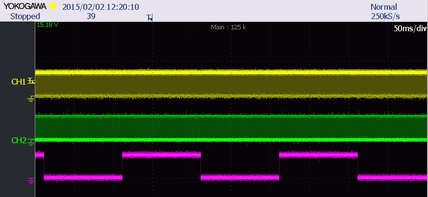
In the following picture, channel 1 and 2 are CH1 and CH1x respectively, and channel 3 is the pulses generated by GPIO_ToggleBits(GPIOD, GPIO_Pin_12) I added before the switch command.
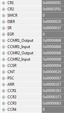
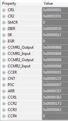
 I attached some pictures to show the register values, and you can see the register changed accordingly, but the output of CH1 and CH1x didn't change at all.before TIM_CCxCmd(TIM1, TIM_Channel_1, TIM_CCx_Enable); TIM_CCxNCmd(TIM1, TIM_Channel_1, TIM_CCxN_Disable);CCER = 0x4
 after TIM_CCxCmd(TIM1, TIM_Channel_1, TIM_CCx_Enable); TIM_CCxNCmd(TIM1, TIM_Channel_1, TIM_CCxN_Disable);CCER = 0x1;
- Mark as New
- Bookmark
- Subscribe
- Mute
- Subscribe to RSS Feed
- Permalink
- Email to a Friend
- Report Inappropriate Content
2015-02-01 11:36 PM
I asked you for *all* TIM1 registers' content. TIM1 (and TIM8) has more registers than other timers.
> CR2 == 0x3F01 Do you understand the implications of this, especially the CCPC bit being set? JW- Mark as New
- Bookmark
- Subscribe
- Mute
- Subscribe to RSS Feed
- Permalink
- Email to a Friend
- Report Inappropriate Content
2015-02-02 5:20 PM
Thank you so much for pointing out CCPC. I should have read the manual more carefully. Now everything works fine. Thank you very very much.
- HRTIM activates output immediately when re-enabled rather than on compare match in STM32 MCUs Products
- Hello, the STM32F030C8T6 chip I recently bought has repeatedly reset after the burning program, and can only be burned once. After the first successful burning, after the reset by external keys, the chip reset pin will continue to output triangle waves, r in STM32 MCUs Products
- Most effective way to generate waveform? in STM32 MCUs Products
- STM32F334 - Peak Current Mode Control/Cycle-by-Cycle Current Limiting in STM32 MCUs Products
- HAL_UART_Transmit_DMA issues in STM32 MCUs Embedded software