- STMicroelectronics Community
- STM32 MCUs
- STM32 MCUs Products
- Re: LCD and FSMC
- Subscribe to RSS Feed
- Mark Topic as New
- Mark Topic as Read
- Float this Topic for Current User
- Bookmark
- Subscribe
- Mute
- Printer Friendly Page
LCD and FSMC
- Mark as New
- Bookmark
- Subscribe
- Mute
- Subscribe to RSS Feed
- Permalink
- Email to a Friend
- Report Inappropriate Content
2008-09-07 7:50 AM
LCD and FSMC
- Mark as New
- Bookmark
- Subscribe
- Mute
- Subscribe to RSS Feed
- Permalink
- Email to a Friend
- Report Inappropriate Content
2011-05-17 3:44 AM
Did somebody use FSMC to drive LCD in Motorola 6800 mode eg. with controllers HD44780 or KS0108 and checked it if this works?
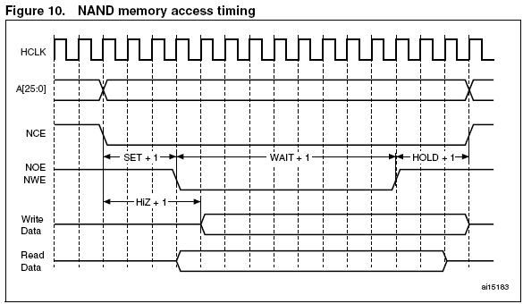
It is possible to use NAND gate to transform Intel 8080 into Motorola 6800 but in Application note TFT LCD interfacing with the high-density STM32F10xxx FSMC, ST wrote that it is possible to use negated NEx signal as E. I'm not sure if timings are correct for this? Did somebody check it? [ This message was edited by: jaroslaw.oska on 07-09-2008 20:21 ]- Mark as New
- Bookmark
- Subscribe
- Mute
- Subscribe to RSS Feed
- Permalink
- Email to a Friend
- Report Inappropriate Content
2011-05-17 3:44 AM
Don't use FSMC parts yet - however offer this analysis:
a) The ''E'' strobe width for both 44780 & 0107/0108 should be 400nS. (these ''are'' 20-25 year old chips) b) The RS & R/W sigs. must be set ''prior'' to the positive transition of ''E'' - not at the same time. c) Eight bit data is latched into both Lcd Cntlrs on the falling edge of ''E.'' d) Beware_1 - clearing a 44780/similar will cause the lcd to ''go busy'' for milliseconds. You have to allow for this. e) Beware_2 - most normal transactions cause a 40uS ''execution time.'' Data sent during execution will be missed or received in error. 20 years ago we could tie a 6800/8051 D-Bus directly to these Lcd Cntlrs and only pay attention to ''delaying'' the E strobe until after RS/RW had stabilized. We could write (or read) to the Lcd using a ''single'' instruction - taking advantage of the automatic, proper generation of RS, RW, and E. *** One trick I noted was to NOT tie the 8051's R/W signal to the Lcd's RW. (that violates the RW set-up time) Simply use one of the low order Adr. bits to control RW - when the bit is low you're writing. This works because the address bits stabilize prior to the onset of the WR strobe. If you can dynamically ''cripple'' the high speed FSMC so that: a) E strobe is 400+ nS b) RS, RW stable prior to E c) 8 bit data stable during E fall d) allow for Lcd's 40uS execution time (normal write) e) allow for Lcd's 1mS+ busy after a ''clear'' (01H) you should be ok.- Mark as New
- Bookmark
- Subscribe
- Mute
- Subscribe to RSS Feed
- Permalink
- Email to a Friend
- Report Inappropriate Content
2011-05-17 3:44 AM
Hi,
Hi, Thanks a lot I did similar investigation. I it possible to use NAND gate mode and get more than I need for this chip. The only need is to use NAND gate to transform WR,RD into E. And we have 256 cycles of HCLK (3.5us) for hold, wait and setup time. I think this will work but I can not have a possibility to check it before PCB.
- Mark as New
- Bookmark
- Subscribe
- Mute
- Subscribe to RSS Feed
- Permalink
- Email to a Friend
- Report Inappropriate Content
2011-05-17 3:44 AM
Hi back,
Your figure summarizes your objectives nicely. A few cautions: a) ''E'' generation - you want this to be qualified by ''both'' NCE and NWR - only when both of these go low will ''E'' strobe high. For safety I suggest that you start this pulse around 500 or so nS. (as you gain confidence you can shorten it) You must guard against this strobe occuring illegally - you will see garbage on the screen when this happens. b) All of these displays must be initialized - often the first such instructions must have ''extreme'' delays (40-100 mS) - be sure to comply. c) Be sure ''not'' to tie the micro's NWE to the displays R/W line. (will violate RW set-up time) d) To avoid the insertion of variable time-delays you may choose to ''read'' the display's ''busy-flag.'' In this way you insure the fastest data transfer to the screen - important when you move up to larger, more pixel intensive screens. (tft-color) Your read of the ''busy'' may capture your processor for 1.6mS (worse case) after a display clear. e) Not required - but use of PWMs to control Contrast and Led backlight brightness saves pots, their space and adds utility. [ This message was edited by: jj.sprague on 06-09-2008 23:54 ]- Mark as New
- Bookmark
- Subscribe
- Mute
- Subscribe to RSS Feed
- Permalink
- Email to a Friend
- Report Inappropriate Content
2011-05-17 3:44 AM
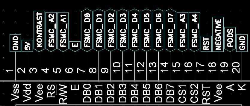
I post schematic diagram, as you can see I use addresses lines to set RS, RW and other control signals. I hope to have only one instruction to control the display.
I will give you information if I will have a success :)

- Mark as New
- Bookmark
- Subscribe
- Mute
- Subscribe to RSS Feed
- Permalink
- Email to a Friend
- Report Inappropriate Content
2011-05-17 3:44 AM
Very nice drawing. Have concern that ''NWE'' and ''NOE'' (which are nand'ed to form positive going ''E'' strobe) are NOT qualified by an address decode - thus you will generate ''E'' illegally!
Sorry if I've missed something - we used to generate unique address - decode it - and then gate that adr. decode with WR or RD to produce ''E.'' That unique adr. decode is what I don't yet see/understand in your drawing. Trying to prevent you from a hacked pcb... Your goal of a ''single'' instruction display write will take our FSMC ''Forward to the Past!'' (way neater than: 1) present RS, RW; 2) present latched data; 3) strobe E high; 4) take E back low - this tired way is so inefficient/uninspired...) [ This message was edited by: jj.sprague on 07-09-2008 15:06 ]- Mark as New
- Bookmark
- Subscribe
- Mute
- Subscribe to RSS Feed
- Permalink
- Email to a Friend
- Report Inappropriate Content
2011-05-17 3:44 AM
Quote:
Have concern that ''NWE'' and ''NOE'' (which are nand'ed to form positive going ''E'' strobe) are NOT qualified by an address decode - thus you will generate ''E'' illegally! Thanks for showing me that problem. I thought that FSMC generate WR/RD signal only if I write or read form addresses of memory that belongs to FSMC. Now, I understand why ST uses hardware NE1 as chip select. I will reconsider this solution (try to explain my boss that is not worth to do that) and maybe back to the standard solution - steering all signals using GPIO. Do you think it is worth to do that using FSMC? [ This message was edited by: jaroslaw.oska on 07-09-2008 16:35 ]- Mark as New
- Bookmark
- Subscribe
- Mute
- Subscribe to RSS Feed
- Permalink
- Email to a Friend
- Report Inappropriate Content
2011-05-17 3:44 AM
1) Possible, Illegal Lcd ''E'' strobe generation:
My firm does not have an FSMC device yet - all my work with you is from FSMC reading/theory - I am highly experienced with displays. I continue to believe that you will be safer to ''better'' qualify your ''E'' strobe - so that only an ''exact'' pair or limited range of addresses will trigger. It may be possible to create a rare, extreme address - and decode it with simple and/or gate. (I recommend this - don't stuff the parts if my illegal E hunch is wrong) 2) FSMC worth it? FSMC swells your board, costs more, may complicate emi/rfi - I would not use it for ''just'' simple displays. Was hoping that FSMC could serve as a conventional ''TFT frame buffer'' - so that we could extract our R,G,B buffer contents and ''paint'' our TFT. Alas - FSMC not fast, capable enough. (driving a TFT with ''controller'' - a la Ap Note - is counter productive imho.) If you really need bulk, fast SRam or high speed read from bulk flash - that would justify FSMC again imho. 3) Alternative to FSMC: How about a ''universal'' (parallel, spi, i2c) asic which ties directly to bulk sram/flash - AND directly/properly drives ''uncontrolled TFT?'' This saves the cost of FSMC - allows you to use one basic STM32 and ''add as needed.''- Mark as New
- Bookmark
- Subscribe
- Mute
- Subscribe to RSS Feed
- Permalink
- Email to a Friend
- Report Inappropriate Content
2011-05-17 3:44 AM
Thanks a lot for help, I will reconsoder my idea.
- External Memory Byte Access in STM32 MCUs Products
- 240x240 Round display with GC9A01A driver using 8-bit 8080 interface in STM32 MCUs TouchGFX and GUI
- FSMC Connection in STM32 MCUs Products
- Interfacing a RGB Display with STM32F407 in STM32 MCUs Products
- SSD1963 with STM32F407 using FSMC in STM32 MCUs Products