- STMicroelectronics Community
- STM32 MCUs
- STM32 MCUs Products
- How to calculate supported external SRAM size for ...
- Subscribe to RSS Feed
- Mark Topic as New
- Mark Topic as Read
- Float this Topic for Current User
- Bookmark
- Subscribe
- Mute
- Printer Friendly Page
How to calculate supported external SRAM size for STM32L Microcontroller ?
- Mark as New
- Bookmark
- Subscribe
- Mute
- Subscribe to RSS Feed
- Permalink
- Email to a Friend
- Report Inappropriate Content
2018-07-10 6:55 AM
- Mark as New
- Bookmark
- Subscribe
- Mute
- Subscribe to RSS Feed
- Permalink
- Email to a Friend
- Report Inappropriate Content
2018-07-10 8:00 AM
Determine if you are going to use an 8-bit or 16-bit data bus, and then look at how many address bit you're using
Up vote any posts that you find helpful, it shows what's working..
- Mark as New
- Bookmark
- Subscribe
- Mute
- Subscribe to RSS Feed
- Permalink
- Email to a Friend
- Report Inappropriate Content
2018-07-11 2:41 AM
Thanks for a quick response here.

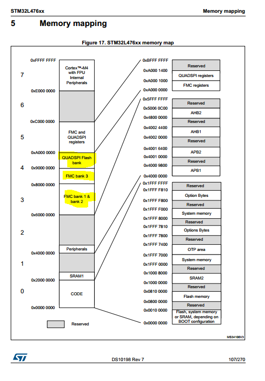
as per this memory mapping diagram below is to consider maximum SRAM calculation.
For FMC Bank 3
0x1000 0000 address available
AddressLine is 16 bit
Dataline is 16bit
Now how I can calculate total supportable SRAM?
- Mark as New
- Bookmark
- Subscribe
- Mute
- Subscribe to RSS Feed
- Permalink
- Email to a Friend
- Report Inappropriate Content
2018-07-11 10:30 AM
Depending on the bank you're looking at 64MB or 256MB, probably more than you can afford to implement externally.
It's is likely to also be constrained by the pins available on the specific device you're using, and you don't specify that.
You also don't really specify what you're attempting to achieve in your design, and that's going to drive appropriate chip choices.
Up vote any posts that you find helpful, it shows what's working..
- Mark as New
- Bookmark
- Subscribe
- Mute
- Subscribe to RSS Feed
- Permalink
- Email to a Friend
- Report Inappropriate Content
2018-07-13 9:49 AM
I am going to use STM32L476VGT6 Controller, Now I need to calculate how much external SRAM memory can be interfaced with
STM32L476VGT6
.I am going to use 16 data lines.
0x10000000 address available and data bits is 16.
For memory calculation
= 0x10000000 x 16 (0x10000000 converted to decimal)
= 268435456 x 16
= 4294967296 bits
= 4194304 Kbits
= 512 MBytes
So we can add up to 512MB SRAM external to
STM32L476VGT6.
Please Correct me if something wrong calculation is done.
- Mark as New
- Bookmark
- Subscribe
- Mute
- Subscribe to RSS Feed
- Permalink
- Email to a Friend
- Report Inappropriate Content
2018-07-13 10:42 AM
As I said before the banks are 64MB and 256MB wide. With the right techniques I could interface 10's of GB, or more, RAM to the L4 part.
Ok, but people don't put that much SRAM externally because it's the most expensive way to do it. I'm thinking you're cheap, or tightly budget constrained.
Why do you need a shed load of SRAM for this application?
Would SDRAM be a more appropriate technology?
Does the L4/L4+ support SDRAM?
Does the L4+ support HyperRAM?
I think the STM32L4R9I-DISCO demos to Octo-SPI
Up vote any posts that you find helpful, it shows what's working..
- STM32CubeIde inline assembler error in STM32CubeIDE (MCUs)
- X-CUBE-EEPROM adding zeros randomly to current page in STM32 MCUs Wireless
- Power consumption of STM32H5 MCU for VIO Pins in STM32 MCUs Products
- Using DMA to create a bit stream with a TIMER on PWM mode in STM32 MCUs Products
- CubeMX 6.16.0: Headless installation in Docker (Ubuntu 24.04) fails in STM32CubeMX (MCUs)