- STMicroelectronics Community
- STM32 MCUs
- STM32 MCUs Products
- External ADC to STM32F7 discovery with 24Bit-SPI i...
- Subscribe to RSS Feed
- Mark Topic as New
- Mark Topic as Read
- Float this Topic for Current User
- Bookmark
- Subscribe
- Mute
- Printer Friendly Page
External ADC to STM32F7 discovery with 24Bit-SPI in DMA
- Mark as New
- Bookmark
- Subscribe
- Mute
- Subscribe to RSS Feed
- Permalink
- Email to a Friend
- Report Inappropriate Content
2018-01-04 3:42 PM
- Mark as New
- Bookmark
- Subscribe
- Mute
- Subscribe to RSS Feed
- Permalink
- Email to a Friend
- Report Inappropriate Content
2018-01-05 5:49 AM
What ADC?
Why do you toggle NSS, once your SPI is slave?
JW
- Mark as New
- Bookmark
- Subscribe
- Mute
- Subscribe to RSS Feed
- Permalink
- Email to a Friend
- Report Inappropriate Content
2018-01-05 9:33 AM
Hello,
I connected the TI device ADS127l01 to the STM32F7. The output of the ADC is configured in Master mode frame sync with MCLK=4MHz, fdata=15kHz, sclk=500kHz. The ADC output signal is a bit like a ''1channel 32Bit I2S''-data, with sync on 15th bit.
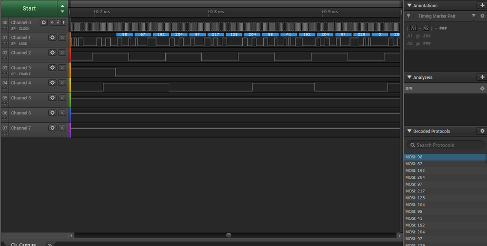
The NSS is just toggeld for debug. This is to see the data in the logic analyzer starting on a user button. Below is the SPI data measured with a logic analyzer ( Channel 0 = sclk, 1 = MOSI, 2=Frame sync, 3 = NSS, 4 = debog out).
The channel 4 debug out is an GPIO output toggled, always when the frame sync Interrupt handler void EXTI2_IRQHandler(void){} is entered.
This is not synced to the frame rising edge. Maybe this is part of the problem. Again it is a DC voltage at the input of the ADC, which should give { 255, 255, 255, xxx}.
Is it the right way to sync on the frame signal with an GPIO-interrupt?

Kind regards
- Mark as New
- Bookmark
- Subscribe
- Mute
- Subscribe to RSS Feed
- Permalink
- Email to a Friend
- Report Inappropriate Content
2018-01-08 11:58 AM
Please describe the channels in terms of the ADC pin names (where applicable).
Looking at Fig.3 in ADC's DS, you want to start SPI on the rising edge of FSYNC, within less than half a SCK time, which is 1us at 500kHz. If ch4 is generated from ch2 by togging a pin in EXTI interrupt, on a F7, lagging some 10us and jittering several us, you are clearly far from that goal. Even if you get rid of the HAL fluff, switch on optimization and run it on the 'F7 raging at hundreds of MHz, if there are other tasks which may interfere, it would be a risk to do this start in software. You may start later, but the delay must be consistent, jitter significantly below SCK period. That calls for hardware to accomplish this.
As SPI can't start on external stimulus natively, AFAIK, you can either devise a timer_capture-triggered-DMA loading SPI's control register to do the start, or - as you've remarked - try to use the SPI in I2S mode (that assumes to have the frame signal connected to WS pin).
The displayed waveform is clearly far from any resemblance of xxFFFFFF, so you probably have some work around the ADC to do, too.
JW
- Mark as New
- Bookmark
- Subscribe
- Mute
- Subscribe to RSS Feed
- Permalink
- Email to a Friend
- Report Inappropriate Content
2018-01-11 9:08 AM
Hello!
Thank you very much for your comments. I will try to use the SPI interface in I2S mode. This will take me some time to do the hardware changes.
On the software side I am still a bit unsure about how to save the data coming from the SPI/ I2S interface.
Is it beneficial to use for the DMA transfer both the half complete HAL_SPI_RxHalfCpltCallback() and complete HAL_SPI_RxCpltCallback() callback function of the HAL?
In a time critical application, it generally makes sense to save the 2 half words, but I am not sure if this is important in practice.
Regards
- Mark as New
- Bookmark
- Subscribe
- Mute
- Subscribe to RSS Feed
- Permalink
- Email to a Friend
- Report Inappropriate Content
2018-04-16 1:06 PM
Hello everybody!
It has been a while since this thread has been active, which was basically about how to connect the Sigma Delta ADC- ADS127L01 to a STM32F7 for high performance signal conversion.
I would like to share some of my findings here, especially on the STM32 Serial Audio interface for somebody who also likes to dive into this topics.
The hardware configuration of the ADS127L01 is in Frame sync slave mode. I daisy-chained two ADCs, which gives an interface quite close to an I2S-Interface with 24Bit data size.
The STM32F7 is connected with its SAI in Master mode delivering the Bitclock and LRclock(Frame sync) to the ADC. The Masterclock (MCLK) is generated by a 12.288MHz crystal oscillator and connected to the ADC and the STM32F7 RCC audio clock input. The SAI clock selection is set to the RCC_SAIxCLKSOURCE_PIN. Important here was, that I had to generate the MCLK also by the STM32F7, even I DO NOT use it further. This is necessary to be able to set the Bitclock different from the MCLK.
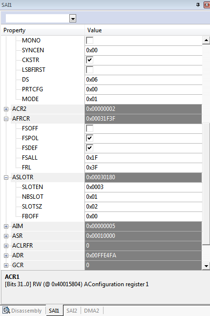
The LRclock is 48kHz and the Bitclock of 6.1MHz is set with a frame length of frl=63.
Here is an example of an I2S connection with a data size of 20Bit:

The interface of the ADC ? ADS127L01 is a bit different:
FSOffset: LeftJustified, the data is clocked out with frame sync
Clock strobing: Rising edge of Bitclock is synced to frame
FSPolarity: Active high
With this settings finally the configuration was fine and the ADC is doing a wonderful job.
The following shows my register settings of the SAI and the measurement of the communication with a logic analyzer.

Regards
- Mark as New
- Bookmark
- Subscribe
- Mute
- Subscribe to RSS Feed
- Permalink
- Email to a Friend
- Report Inappropriate Content
2023-11-12 2:10 AM
Hello Kerry King !
I am attempting to develop a condition based monitoring system for a marine vessel. We have four engines to monitor & record vibration data. Need help with integrating the ADS127l01-Evaluation Kit with STM32 to convert the SPI to CAN data and daisy chain all four engines. Once done, data needs to be saved on a LOGGER / similar, for analysis later. I see you have already gone through that phase; perhaps you could help, kindly.
I look forward to hearing from you and any other friend who could contribute.
Sincerely,
Jawad
- USB OTG HS Host: PENA cleared spuriously at HFNUM=16383 with ULPI PHY (USB3300) in STM32 MCUs Embedded software
- STM32H757 SDMMC + FATFS consistently returns FR_NOT_READY in STM32 MCUs Embedded software
- Stm32h743iit6 preload at boot image background using LibJPeg in STM32 MCUs Embedded software
- PWM input output drift in STM32 MCUs Products
- STM32G431 Bootloader issue in STM32 MCUs Products
