Turn on suggestions
Auto-suggest helps you quickly narrow down your search results by suggesting possible matches as you type.
Showing results for
- STMicroelectronics Community
- STM32 MCUs
- STM32 MCUs Embedded software
- Re: stm32f429i-discovery SDRAM HAL driver assistan...
Options
- Subscribe to RSS Feed
- Mark Topic as New
- Mark Topic as Read
- Float this Topic for Current User
- Bookmark
- Subscribe
- Mute
- Printer Friendly Page
stm32f429i-discovery SDRAM HAL driver assistance
Options
- Mark as New
- Bookmark
- Subscribe
- Mute
- Subscribe to RSS Feed
- Permalink
- Email to a Friend
- Report Inappropriate Content
2015-07-14 5:17 PM
Posted on July 15, 2015 at 02:17
I can't seem to find a single example using the HAL driver. I am wondering what is the suggested solution for address management for the SDRAM and also, what is the start address anyway and how do you know?
#hal #!stm32f4-disco #sdram
Labels:
- Labels:
-
STM32Cube MCU Packages
3 REPLIES 3
Options
- Mark as New
- Bookmark
- Subscribe
- Mute
- Subscribe to RSS Feed
- Permalink
- Email to a Friend
- Report Inappropriate Content
2015-07-14 8:37 PM
Posted on July 15, 2015 at 05:37
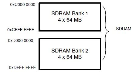
It's a secondary bank SDRAM so it lives at 0xD0000000 on the DISCO. The EVAL series board (STM324x9I-EVAL) it's the primary bank at 0xC0000000
For HAL code perhaps review some of the examples might help STM32Cube_FW_F4_V1.3.0\Projects\STM32F429I-Discovery\Examples\FMC\FMC_SDRAM\Src\main.c
Tips, Buy me a coffee, or three.. PayPal Venmo
Up vote any posts that you find helpful, it shows what's working..
Up vote any posts that you find helpful, it shows what's working..
Options
- Mark as New
- Bookmark
- Subscribe
- Mute
- Subscribe to RSS Feed
- Permalink
- Email to a Friend
- Report Inappropriate Content
2015-07-15 2:07 AM
Posted on July 15, 2015 at 11:07
Thanks for the reply.
So according to the settings I can see in the example, the row address is 12bit, the column address is 8bit and there are 4 banks. 16 * 2^12 * 2^8 * 4 = 67108864 right?I've actually looked at that example, it does not use the read and write functions from the HAL driver but rather writes directly using a pointer to the memory. But that's OK.In order to calculate the address the bank address (0xD0000000) is multiplied by WRITEÖ¹_READÖ¹_ADDR (0x800) and by uwIndex (32bit) multiplied by 4.So this bank address is the starting address of the SDRAM, right?I'm not sure what is the write_read_address?I'm also not sure why uwIndex is multiplied by 4?Last, how do you know what is the start address for the external RAM? It is larger than the physical address that can be addressed using the available bits.Options
- Mark as New
- Bookmark
- Subscribe
- Mute
- Subscribe to RSS Feed
- Permalink
- Email to a Friend
- Report Inappropriate Content
2015-07-15 5:12 AM
Posted on July 15, 2015 at 14:12
I've basically read and understood the manuals.
The Cortex-M4 has a 32-bit address bus, giving it access to a 4GB address space. The SDRAM lives *within* this address space, the chip select in the logic surrounding the core recognizes the 256KB region between 0xD0000000..0xDFFFFFFF. The logic basically decodes, recognizes, the 0xD value in the high order 4-bits of the address on the bus, and directs traffic to the FMC/SDRAM. I'm not familiar with WRITE?_READ?_ADDR(), is suspect it multiplies by 4 because you're accessing 32-bit words, which take 4-bytes, which are separate but contiguous within the memory space. The memory map is described in the FMC/FSMC section of the REFERENCE MANUAL
Tips, Buy me a coffee, or three.. PayPal Venmo
Up vote any posts that you find helpful, it shows what's working..
Up vote any posts that you find helpful, it shows what's working..
Related Content
- STM32 Virtual COM Port "Unknown USB Device" on one particular laptop in STM32 MCUs Boards and hardware tools
- STM32L031 RTC Wake up interrupt service routine never entered in STM32 MCUs Embedded software
- Need Help with Developing GT2931 Goodix Touch Controller Driver on STM32 in STM32 MCUs Boards and hardware tools
- Need Help with Developing GT2931 Goodix TouchGFX Controller Driver on STM32 in STM32 MCUs TouchGFX and GUI
- Motor Control Support in STM32 MCUs Motor control