- STMicroelectronics Community
- MEMS and sensors
- MEMS (sensors)
- the gerber files of STEVAL-MKI181V1 is wrong , the...
- Subscribe to RSS Feed
- Mark Topic as New
- Mark Topic as Read
- Float this Topic for Current User
- Bookmark
- Subscribe
- Mute
- Printer Friendly Page
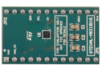
the gerber files of STEVAL-MKI181V1 is wrong , the pin map is for LIS3MDL, not LIS2MDL , please check
- Mark as New
- Bookmark
- Subscribe
- Mute
- Subscribe to RSS Feed
- Permalink
- Email to a Friend
- Report Inappropriate Content
2020-06-12 4:44 AM
the gerber files of STEVAL-MKI181V1 is wrong , the pin map is for LIS3MDL, not LIS2MDL , please check
- Mark as New
- Bookmark
- Subscribe
- Mute
- Subscribe to RSS Feed
- Permalink
- Email to a Friend
- Report Inappropriate Content
2020-06-12 9:14 AM
- Mark as New
- Bookmark
- Subscribe
- Mute
- Subscribe to RSS Feed
- Permalink
- Email to a Friend
- Report Inappropriate Content
2020-06-12 3:49 PM
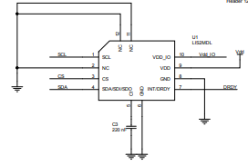
schematic is right but the gerber file is not for LIS2MDL, I found this issue after my PCB back which use the gerber file .
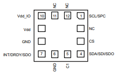
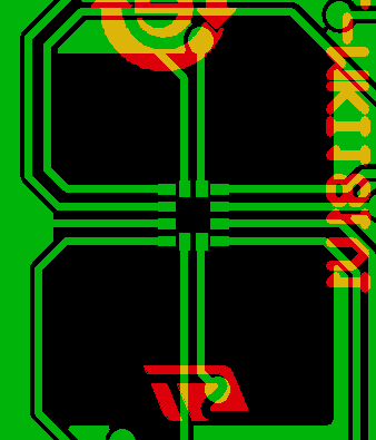
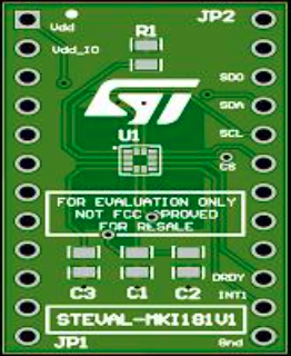
one simple way to check : PIN3 in the PCB layout had been connect to GND
the picture is not the same like the EVAL board of MKI181V1
it is like this
thanks.
- Mark as New
- Bookmark
- Subscribe
- Mute
- Subscribe to RSS Feed
- Permalink
- Email to a Friend
- Report Inappropriate Content
2020-06-16 1:19 AM
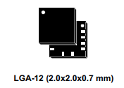
Hi @Junger , I was focusing on the device footprint and not on the signal routing. I now understand what you do mean. The chip is also soldered rotated with respect to the pin1 of the gerber files on the STEVAL-MKI181V1. The fact is that usually this is an ST internal matter since the STEVAL boards are sold whit chips already mounted on them... But I will report this issue internally. Regards
