- STMicroelectronics Community
- Product forums
- Interface and connectivity ICs
- [STUSB4500] Can I remove the typical circuit on ST...
- Subscribe to RSS Feed
- Mark Topic as New
- Mark Topic as Read
- Float this Topic for Current User
- Bookmark
- Subscribe
- Mute
- Printer Friendly Page
[STUSB4500] Can I remove the typical circuit on STUSB4500's VBUS_VS_Disch pin?
- Mark as New
- Bookmark
- Subscribe
- Mute
- Subscribe to RSS Feed
- Permalink
- Email to a Friend
- Report Inappropriate Content
2020-12-15 10:30 PM
Hello,
In the STUSB4500 datasheet, there are 2 typical circuits. Both of them include a circuit for the VBUS_VS_Disch pin. Components are D4, C4, R1 and R4. Based on the information in the datasheet, this circuit should be here to limit the discharge current to 50mA. Moreover, this pin is used by the chip to sense vbus voltage.
What's the purpose of the diode D4?
Discharge feature is optional and can be disabled in NVM. I want to disable it in my application, do I still need to link VBUS_VS_Disch to VBUS to sense VBUS? If so, what is the minimal circuit, do I need some resistors?
Thanks,
Arthur
- Mark as New
- Bookmark
- Subscribe
- Mute
- Subscribe to RSS Feed
- Permalink
- Email to a Friend
- Report Inappropriate Content
2020-12-16 6:17 PM
When VBUS is charging up, D4 switches ON and charges the capacitor.
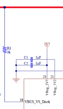
The minimal circuit for VBUS_VS_Disch would be:
- Mark as New
- Bookmark
- Subscribe
- Mute
- Subscribe to RSS Feed
- Permalink
- Email to a Friend
- Report Inappropriate Content
2020-12-16 10:11 PM
Thanks for sharing the minimal circuit.
Just for my understanding, in the initial typical circuit, what's the purpose of the circuit with C4, D4 and R1? Is it some sort of protection because VBUS will sense the capacitor voltage instead of VBUS directly?
Are R1 and R4 a voltage divider? Or R1 is here to "finish" C4 charging when diode is switching off?
Thank you,
Arthur
- Mark as New
- Bookmark
- Subscribe
- Mute
- Subscribe to RSS Feed
- Permalink
- Email to a Friend
- Report Inappropriate Content
2020-12-16 10:37 PM
They are the VBUS discharge circuit.
When VBUS is charging up, D4 switches ON and charges the capacitor in a very short time.
The fluctuations in VBUS will be filtered by the C4 and R1.
The voltage is monitored with R4.
During there is a significant drop in the VBUS (cable disconnection, power down transitions, hard reset and error recovery state), the VBUS discharge path is activated on the VBUS_VS_Disch pin.
- Mark as New
- Bookmark
- Subscribe
- Mute
- Subscribe to RSS Feed
- Permalink
- Email to a Friend
- Report Inappropriate Content
2020-12-17 12:38 PM
Oh ok, R1 and C4 act as a filter. Without D4, the capacitor C4 will take too much time to charge up that's why we need the diode right?
- Mark as New
- Bookmark
- Subscribe
- Mute
- Subscribe to RSS Feed
- Permalink
- Email to a Friend
- Report Inappropriate Content
2020-12-20 8:47 PM
Yes. We need it charged rapidly ; as well as discharged at a controlled speed. A diode fits the need perfectly.
- STUSB4500 Reference Design using STL6P3LLH6 in Power management
- STUSB4500 Repeated Component Failure in Power management
- STUSB4500 not triggering higher PD voltage – VBUS_READY remains false in Power management
- STUSB4500 IC failure in the field in Others: hardware and software
- USB-C PD: STUSB4500 FTP_KEY changable? in Others: hardware and software
