Turn on suggestions
Auto-suggest helps you quickly narrow down your search results by suggesting possible matches as you type.
Showing results for
- STMicroelectronics Community
- Product forums
- Analog and audio
- PCB routing of inner balls for 400um flip-chip pac...
Options
- Subscribe to RSS Feed
- Mark Topic as New
- Mark Topic as Read
- Float this Topic for Current User
- Bookmark
- Subscribe
- Mute
- Printer Friendly Page
PCB routing of inner balls for 400um flip-chip package on TS4621ML
Options
- Mark as New
- Bookmark
- Subscribe
- Mute
- Subscribe to RSS Feed
- Permalink
- Email to a Friend
- Report Inappropriate Content
2014-04-16 3:24 PM
Posted on April 17, 2014 at 00:24 Thanks,Jeff
Hi I have a question concerning the PCB routing of the TS4621ML headphone amplifier in 400um flip-chip package.
I have the STEVAL-CCA025V1 demoboard for the TS4621E part and looking at the gerber files for it it appears the inner balls of the package were routed by placing a via directly next to the ball pad but this would seem to violate the design guidelines in the datasheet for the part (which recommend a max 100um track from the pad). I'd like to avoid using microvias due to cost and would thus like to receive some guidance concerning routing the inner balls of this package.Here is a screenshot of the gerbers for the demoboard to show what I'm talking about: Thanks,Jeff
Labels:
- Labels:
-
Audio Amplifiers
This discussion is locked. Please start a new topic to ask your question.
6 REPLIES 6
Options
- Mark as New
- Bookmark
- Subscribe
- Mute
- Subscribe to RSS Feed
- Permalink
- Email to a Friend
- Report Inappropriate Content
2014-04-16 6:47 PM
Posted on April 17, 2014 at 03:47
hello Jeff,
for flip-chip 400um package , due to clearance between two solder pads is around 180um, then if you need to route trace in top layer, it was very difficult and risky . please find application note for this package in below link. ThanksOptions
- Mark as New
- Bookmark
- Subscribe
- Mute
- Subscribe to RSS Feed
- Permalink
- Email to a Friend
- Report Inappropriate Content
2014-04-17 2:50 AM
Posted on April 17, 2014 at 11:50
Zhao Yun,
Thanks for the reply. I've read that app note and it doesn't really give any routing guidelines for the inner balls other then suggestion using micro vias as an ''alternative''.I'm mainly wondering what was done on the demoboard http://www.st.com/web/en/catalog/tools/PF250873 as show in the posted image I gave. It looks like they just put vias right next to the inner ball pads. Is that a recommended procedure?JeffOptions
- Mark as New
- Bookmark
- Subscribe
- Mute
- Subscribe to RSS Feed
- Permalink
- Email to a Friend
- Report Inappropriate Content
2014-04-17 3:22 AM
Posted on April 17, 2014 at 12:22
hello Jeff,
yes, it's recommended routing for inner balls fan out since the solder pads diameter for BGA balls is around 0.25mm , then if we used buried micro via, the drill diameter will be much less than 0.25mm , and processing cost will be increased as you mentioned before. if we shifted via posistion and just next the pads, it will be improved. you could consider to use 0.3mm diameter via with 0.2mm drill hole for inner ball soldering pads fanout. ThanksOptions
- Mark as New
- Bookmark
- Subscribe
- Mute
- Subscribe to RSS Feed
- Permalink
- Email to a Friend
- Report Inappropriate Content
2014-04-18 8:08 AM
Posted on April 18, 2014 at 17:08Zhao Yun,Thank you very much for the recommendations. I'm glad to hear I can avoid using micro vias with this part to save cost. I appreciate your help.Jeff
Options
- Mark as New
- Bookmark
- Subscribe
- Mute
- Subscribe to RSS Feed
- Permalink
- Email to a Friend
- Report Inappropriate Content
2014-04-24 3:49 PM
Posted on April 25, 2014 at 00:49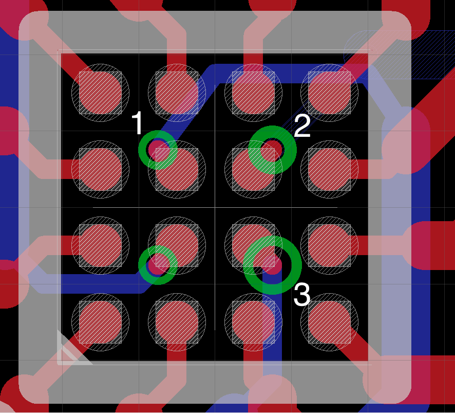
Zhao Yun,
Hi, I finished the layout for this board and followed your recommendations for the breakout of the inner pads of the 400 um bga however I think they are too large.If you look at the screenshot, number 3 is your recommendation, 8mil (.2mm) drill and 12mil via pad (.3mm). As you can see this looks quite large as does the drill clip a good portion of the bga pad and the ring percentage is small. Number 2 is a 5mil (.127mm) drill and 10mil (.254mm) via pad. Number 1 is a 5mil (.127mm) drill and 8mil (.2mm) via pad. Number 1 looks more like what is on your eval board however I worry about the annular ring being too small. Number 2 was increasing the via pad size a bit.Do you know in the eval board exactly what via pad and drill size is used? Based on this picture do you have different recommendation? Thanks,Jeff
Options
- Mark as New
- Bookmark
- Subscribe
- Mute
- Subscribe to RSS Feed
- Permalink
- Email to a Friend
- Report Inappropriate Content
2014-04-24 7:49 PM
Posted on April 25, 2014 at 04:49 hello Jeff, yes , the via size will be large than pads for ball, below is snap shot of demo board layout.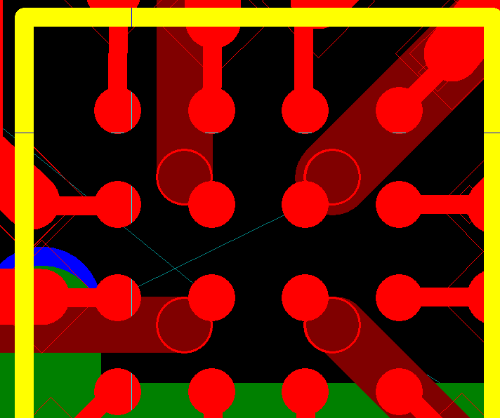 for 5mils drill hole , if it's good balance between cost and reliabilty , you can use it in your PCB design . Thanks
 for 5mils drill hole , if it's good balance between cost and reliabilty , you can use it in your PCB design . Thanks