Join conversations with your peers and ST experts. Explore the full potential of STM32 microcontrollers for your embedded design.
Most recent activity
Problem:HAL_FLASHEx_Erase returns error 0x20000, and HAL_FLASH_Program does return HAL_OK but does not actually write any data to the flash.Goal: Erase and install new firmware on flash on its own inside the bootloader.I am developing a bootloader for the STM32H533RET6. I have TrustZone enabled, and configured the secure and non-secure regions. I am trying to erase and write to the non-secure part of the flash, from the bootloader which is secure (and separate from the actual application). I have disabled any write protection that I am aware of inside the option bytes. I also use the Memory Management Tool inside CubeMX to configure the secure and non-secure regions. For the non-secure region of the flash I have set "Access Permissions" to "RW by any privilege level". I do have a Flash watermark set on bank 1 but this does not cover any of the non-secure flash regions. No watermark is set on bank 2. Below is the code I use to erase and write to a sector on the flash:uint32_t Erase
Hi,I wanted to use an external voltage reference of +2.048V on the Nucleo Board. To do so I removed SB57 as dictated in UM1724 document: SB57 (VDDA/VREF+)ON VDDA/VREF+ on STM32 is connected to VDD.OFF VDDA/VREF+ on STM32 is not connected to VDD and can be provided frompin 8 of CN5 (Used for external VREF+ provided by ARDUINO® shield) The Absolute Maximum Ratings for STM32F072xB (table 21) give the following:VDD–VDDA Allowed voltage difference for VDD > VDDA - 0.4 V Does this mean I am bound to a 3.3V reference and can not use lower voltages? On Arduino boards these normally accept other voltages.
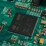
I would like to ask if there has been any change in the screen printing of STM32L433RCT6 from Taiwan, as the Z next to the ARM in the first line is not close, while the Z next to the ARM in China is close. As shown in the following figure.
Hello, While working with STM32F446RET6, I encountered a problem with I2C1. When using HAL_I2C_Mem_Read_IT(), an error occasionally occurs in the form of sending 0x00 instead of the address with the read bit after Repeated Start. The error seems to only occur with O3 optimization. I2C Configuration: NVIC Configuration: Only TIM1 update interrupt (TIM10 not used), DMA1 stream2 (SPI3_RX) and DMA1 stream5 (SPI3_TX) have higher priority than I2C1. Here is an example of a correct signal: The signal with error and I2C_Flush_DR() looks like this: static void I2C_Flush_DR(I2C_HandleTypeDef *hi2c) { /* Write a dummy data in DR to clear TXE flag */ if (__HAL_I2C_GET_FLAG(hi2c, I2C_FLAG_TXE) != RESET) { hi2c->Instance->DR = 0x00U; } } The signal and I2C_Flush_DR() looks li
Hi,Ref.manual (RM0477 Rev 8) in chapter 32.3.3 PSSI clock saysIn case when PSSI transmitting data, then RDY pin is input.Datasheet (DS14360 Rev 2) shows setup and hold time of RDY pin (input) referenced to rising edge as well as data pins (outputs).I think that's a contradiction. So how is it really and to which edge do RDY setup and hold times relate ?Thanks,Michal Dudka
I have successfully run the USB HS Mass storage on a new project without the use of freertos and touchgfx , But when the touchgfx code for STM32H750B-DK is modified to run the code I am getting hard faultsstatic uint8_t usb_done = 0; extern ApplicationTypeDef Appli_state; extern USBH_HandleTypeDef hUsbHostHS; extern FATFS USBHFatFS; extern char USBHPath[4]; void Debug_Print(char *str) { HAL_UART_Transmit(&huart4, (uint8_t*)str, strlen(str), 100); } static uint8_t file_written = 0; void StartDefaultTask(void *argument) { Debug_Print("Task Started\r\n"); for(;;) { USBH_Process(&hUsbHostHS); if (Appli_state == APPLICATION_READY && file_written == 0) { Debug_Print("USB Detected\r\n"); if (USBH_MSC_IsReady(&hUsbHostHS)) { Debug_Print("MSC Ready\r\n"); FRESULT res; FIL file; UINT bw; /* Mount USB */ Debug_Print("Mounting...\r\n"); res = f_mount(&USBHFatFS, USBHPath, 1); if (res == FR_OK) { Debug_Print("Mount OK\r\n"); /* Create
Hello everyone,I am working with the NUCLEO-H723ZG board and attempting to establish Ethernet communication using TCP/IP. The firmware was built and flashed successfully using STM32CubeIDE version 1.19.0.However, I am facing issues with basic network connectivity. Below are the details of my setup and observations:Setup DetailsBoard: NUCLEO-H723ZGIDE: STM32CubeIDE v1.19.0Ethernet stack: LwIPPHY interface: RMIIFlashing tool: ST-LINK (onboard)Test performed: Ping test from PCObserved BehaviorThe Ethernet port LEDs (orange and green) remain solid ON after connecting the Ethernet cable.Ping requests consistently fail (Request timed out).No response is received from the board.Troubleshooting Already PerformedTested both Static IP and Dynamic IP (DHCP) configurations.Verified IP address, subnet mask, and gateway settings.Tried multiple Ethernet cables to rule out cable-related issues.Rebuilt and reflashed the project multiple times.Verified that the firmware flashes successfully and runs wit
Hi everybody,I'm learning to use the ADC in a STM32F411CEU in Continuous Mode and Single Conversion with Polling. When the code is downloaded to the MCU everything runs ok (I mean, when the MCU runs by itself without any ST-Link connected).The problem appears when I try to execute the code in a debugging session. The first time the function HAL_ADC_PollForConversion() is called, the result is HAL_OK, but in the next iterations the functions doesn't return HAL_OK anymore.I know, I know, with Continuous Mode I should be using DMA. But I'm trying to learn the different operation modes (single conversion, scan mode, polling, DMA, etc.)One thing I've found is that if I set the ADC parameter End Of Conversion Selection = EOC flag at the end of all conversions instead of End Of Conversion Selection = EOC flag at the end of single channel conversion , then the function HAL_ADC_PollForConversion() works ok in all the iterations when debugging. Can anybody explain m
Hello everyone,I am currently working on a project using the STM32F030C, and I have a question regarding the GPIO speed configuration (slew rate) for SPI pins.Here is my setup:MCU: STM32F030CInterface: SPI (configured as Slave)SPI Clock Frequency: 13.5 MHzTo keep EMI (Electromagnetic Interference) emissions as low as possible, I was considering setting the GPIO output speed for the SPI pins (specifically MISO, since the MCU is the slave) to GPIO_Speed_Level_Low.However, according to the datasheet (see attached screenshot), the "Low" speed setting is specified for a maximum frequency of 2 MHz.My questions are:Is it practically possible to run a 13.5 MHz SPI signal with the GPIO speed set to Low, despite the datasheet specs?Does this pose a high risk of corrupted/poor communication due to the slew rate being too slow (e.g., degraded signal integrity, failing to meet setup/hold times for the master)?Has anyone here tried this approach to reduce EMI at similar frequencies, or is it strictl
I am trying to create a simple UDP server using the NUCLEO-H743ZI2 board. I will port this to a similar microcontroller in the same family (STM32H750B) once I get it working. I am able to build the example code from this repository: https://github.com/stm32-hotspot/STM32H7-LwIP-Examples/tree/main/STM32H743_Nucleo_ETHIt successfully responds to pings and shows up in my router device list. I used:STM32CubeIDE Version: 1.17.0 STM32Cube FW_H7 Version 1.12.1.Following the instructions in the README, I attempted to build the application from scratch on the NUCLEO board, but I haven't been able to get it to respond to a ping despite a few days of troubleshooting. Can someone tell me if there is something wrong with my configuration file?
Hi, two years ago I posted this thread:Solved: How to set "Don't fragment" flag LWIP short TCP pa... - STMicroelectronics CommunityNow I just was reviewing it for another application that truly needed to send more data and was not allowed to wait 50ms for every sent packet.Final root cause explanationThe 415-byte packets were being ACKed after ~40–50 ms because I was only sending one TCP segment at a time and waiting for it to be acknowledged within my application code, before sending the next one.This behavior is due to the TCP Delayed ACK algorithm implemented by Windows. When Windows receives a single TCP segment smaller than the MSS, it does not immediately send an ACK. Instead, it waits approximately 40–50 ms before acknowledging it.This behavior is described in RFC 1122, section 4.2.3.2 ("When to Send an ACK Segment"), which explains that a TCP implementation may delay sending an ACK in order to reduce protocol overhead.If a second TCP segment is received before the delayed ACK t
Controller: STM32F303ZEWritten a function to read ROM memory as belowvoid ServiceROMRead(tst_ServiceDataset* ptrService){// Variable holds ROM addressDWORD ROMAdd = DIAG_ZERO;// Flag represents JUP service trigger state.RFJupExeFlag = TRUE;// Address from where the data needs to be readROMAdd = ptrService->DataAddr;//Check for the EEPROM addressif((ROMAdd > ROM_ENDADD)) //ROM_ENDADD is 0x0807AFFF{// wrong addressptrService->State = WRONG_DATA;//Indicator for wrong address passed}else{ptrService->ptrData = (BYTE *) ptrService->DataAddr;}}When I pass ptrService->DataAddr as 0x8000020 or 0x8000080 to the above function ServiceROMRead from my application it is sometimes leads to a system resetApplication is placed at 0x08003000 to 0x0807AFFFBootloader is placed at 0x08000000 to 0x08002FFF1. Why is the controller resetting when I try to read ROM from address 0x8000020 or 0x8000080?2. Will trying to read data from address 0x8000020 or 0x8000080
HelloI have a STM32H7R3V8T6 and want to use a few peripherals and GPIOs. However, I don't manage to see an output with my analyzer. The peripherals themselves seem to work: An XSPI receive for example does receive some dummy bytes and takes exactly the required time for the transfer (measured with the cycle counter), but the pins do not show anything.I reduced my code and came up with this simple demonstration of how I initialize a GPIO:int main(void) { SystemCoreClockUpdate(); HAL_Init(); SystemClock_Config(); __HAL_RCC_GPIOB_CLK_ENABLE(); GPIO_InitTypeDef GPIO_InitStruct = {0}; GPIO_InitStruct.Pin = GPIO_PIN_12; GPIO_InitStruct.Mode = GPIO_MODE_OUTPUT_PP; GPIO_InitStruct.Pull = GPIO_NOPULL; GPIO_InitStruct.Speed = GPIO_SPEED_FREQ_LOW; HAL_GPIO_Init(GPIOB, &GPIO_InitStruct); while (1) { HAL_GPIO_TogglePin(GPIOB, 12); HAL_Delay(10); } }The debugger shows that I reach the loop. The registers of the peripheral seem to be correct, but the pin doesn't toggle. This als
I have created a UI in touchgfx designer, after I opened CubeMX and based .ioc file from touchgfx designer generate codes for stm32n6.Now I want to build these codes in Cube IDE but get this Error . Errors occurred during the build.Errors running builder 'CDT Builder' on project 'STM32N6570-DK-FreeRTOS_Appli'.Cannot invoke "com.st.stm32cube.common.mx.registry.IIdeHelper.getRootProject(org.eclipse.core.resources.IProject)" because the return value of "com.st.stm32cube.common.mx.registry.MxRegistry.getIdeHelper()" is null
HI, I am using STM32H745BIT6 ST controller in my custom board.Configured in Direct SMPS mode. When the board is powered on the VCAP voltage is 1.2V and settling at 1V as expected when we try to flash the program to controller the voltage is same, but when we are trying to enter into debug mode the voltage is dipping from 1V to 0.6V and after 5uS its coming back to 1.2V.( Image is attached for reference)Due to this issue, I am not able to enter to debug mode controller is getting disconnected and showing the pop-up as TARGET IS LOST. I have taken all the precautions mentioned in datasheet and reference manual.1) Shorting all three VCAP pins.2) Connected two 2.2uF capacitor near to the pins.3) Even tried with higher capacitor value.4) Checked the shorts in the pins and board with the help of multimeter.5) The PWR_CR3 register is also set to Direct SMPS mode and verified the last 4 bits as 0100.6) Verified in the IOC that it is configured to Direct SMPS
HelloI'm developing on the NUCLEO-N657X0-Q board using the STM32N657X0H3Q.I'm trying to trigger the ADC when the CCR value on CH2 of TIM1 meets the up counter of TIM1. This triggers the ADC conversion. Once the ADC conversion is complete, a callback function is triggered to store the ADC value in a variable. To verify the callback function's operation, I'm trying to toggle the GPIO.When I debug and observe the waveforms, I see the waveforms on CH1 and CH2 of TIM as designed. However, the problem is that the GPIO toggles aren't observed. When I check the ADC values in debug mode, the g_adc_raw value is stuck around 1290 and the g_adc_mv value is stuck around 566. Connecting the ADC pin to GND doesn't return 0.The STM32n6 example, ADC_SingleConversion_TriggerTimer_DMA, works normally, so there seems to be nothing wrong with the board itself.I plan to control the DC-DC converter, so I need to read the value for each ADC conversion and run the controller, so I don't think DMA is necessar
Greetings, I am working with the STM32U585RI and a sensor that asserts an interrupt on the MISO line. I would like to know whether this setup is feasible, and if so, how best to implement it. One approach I have considered is to use a separate pin (LPGPIO) to monitor the interrupt condition and then trigger the SPI sequence. However, during ongoing SPI transactions, I would need to temporarily disable the interrupt feature and re‑enable it after each transaction. My question is, how can this be achieved using LPBAM? Is there a recommended way to configure LPBAM so that the interrupt handling and SPI transfers can coexist without conflict? Any suggestions or guidance would be greatly appreciated. Best regards, Rasool
I am unable to successfully run zephyr samples/bluetooth/peripheral on nucleo_wb55rg. The software appears to enter a fault handler. The basic blinky project does work (samples/basic/blinky) Wireless stack stm32wb5x_BLE_HCILayer_fw.bin v1.24 is programmed and running (see attachments) I have also tried v1.23 without success. Is there a known good combination of software and hardware for stm32 BLE and zephyr?
Hello, We want to use the STMH723ZG with the Motor Control SDK. To do this I cannot find the .json file support for the board in the motor control workbench. Could I use another .json file from one of the fully-supported boards like the H745? Also, we are using custom power electronics + motor setup so to my knowledge our board has sensors it outputs to the stm + it takes a pwm 3-phase input from the stm to spin the motors. What all info do I need and what process do I follow to get a project built for this setup with the motor control SDK.
Вітаю. Створив DC-DC перетворювач на мікроконтролері G4 серії. У я кості регулятора використовую апаратний FMAC, current mode. Моє питання стосується перерегулювання рівня вихідної напруги при старті перетворювача. На борту маю апаратну кнопку вимкнення живлення, а саме фізичне від'єднання акумулятора від перетворювача, а також тактові перемикача для користувача, якими безпосередньо вмикається та вимикається процес перетворення, та налаштування користувачем деяких параметрів. М'який старт програмно не реалізовано. Ситуація наступна, перший пуск перетворювача після увімкнення кнопкою живлення проходить бех перерегулювання, що я можу підтвердити осцилограмами. А ось усі наступні пуски супроводжуються короткотривалим перерегулюванням рівня вихідної напруги. Будьласка, хто має бажання мені допомогти, відгукніться, за запитом надам усю необхідну інформацію. Осцилограми хочу скинути наступним постом.
I read UM3451 (STM32N6xx security guidance for SESIP level 3 certification) chapter 3.2.2 Secure installation and I wonder why aren't the FSBL signature public keys not written into OTP fuses? Only the 8 words (32 bytes) of hashes of all 8 public keys are written by the instructions.Chapter 2.1. Secure boot here in wiki explains that one of 8 active public key hashes in FSBL binary header is compared to the one in OTP and if they match, then "that" public key is trusted. But it doesn't explicitly say where does "that" public key come from.From UM3234 concept drawings (Figure 12-13.) I begin to understand that public key (in some changed form) is provided with the FSBL authentication extension header. So does it mean the MCU does not know the public key and it trusts the provided public key based on the hash table match only?Am I missing something here, but it appears to me that uniqueness of public keys have been heavily reduced. Since each public key hash is individuall
Hello,Is it possible to power this board with an external 3.3 volt supply while still having the st-link active for debugging purposes? If not, how else can I debug my firmware? I've looked through the UM2592 for the dev board, but can't seem to nail down my answer. Any advice is appreciated. Thank you.
Hi,I am testing the ECC on DTCM on the STM32H7A3ZI. At start of day I initialize all of DTCM apart from a single test location. I have a test which reads from that uninitialized location and successfully provokes the SRAM ECC interrupt, correctly reporting the address for the uninitialized location. (I am following application note AN5342).However, I am finding that the same ECC error is raised in other circumstances, when I am confident that my code is not reading the test location. This happens when the IDE is not connected, so it is not the IDE which is reading that location.I have another test that provokes flash ECC errors, and it is currently the code of this test that somehow provokes the SRAM ECC error as well as the flash ECC error. However I don't think this code is reading the uninitialized location (and I have also seen other code provoke the problem). The address reported in the FAR register is always that of my uninitialized test locati
Hello everyoneI am using a Nucleo H7S3L8 evaluation module am I am trying to get some GPIOs and peripherals to work. I have generated a demo project that toggles a few LEDs and that works. Then I started replacing the GPIO ports (A, B, etc.) and pin numbers in order to get other GPIOs to toggle (I left the rest of the code as-is, really just replaced the letters and numbers). However, I didn't manage to get an output on any of the GPIOs belonging to ports O and P. I tried GPIOO 0 and 4 as well as GPIOP 0-3 and attached the analyzer at CN10 13, 15, 19, 21, 23, 25 with GND at CN10 17 (always one at a time). All these signals do not toggle. Other GPIO banks such as GPIOB and GPIOM work.Are the O and P ports different than the others? Do I miss some special settings? I will later be using the XSPI there, so I will need exactly these pins.I appreciate any help!PS Here are my jumper settings:JP1: not connectedJP2: connectedJP3: only STLK connectedJP5: connected to 3.3 VJP6: not connected
// To regenerate crash, follow these steps // In simulator mode // 1. Rotate screen if (touchgfx::HAL::getInstance()->getDisplayOrientation() == touchgfx::ORIENTATION_PORTRAIT) { touchgfx::HAL::getInstance()->setDisplayOrientation(touchgfx::ORIENTATION_LANDSCAPE); } else { touchgfx::HAL::getInstance()->setDisplayOrientation(touchgfx::ORIENTATION_PORTRAIT); } // 2. Go to other screen application().gotoScreen2ScreenCoverTransitionEast(); // CrashThere is probably a bug after rotating screen in simulator mode. Additionally, in debug mode (on hardware) when I apply screen rotation, it is not validated. If I change screen to another one, rotation is applied but with glitches in pixels.
ST Community highlights – April to June 2026
Already have an account? Login
No account yet? Create an account
Enter your E-mail address. We'll send you an e-mail with instructions to reset your password.