
STM32 MCU reference manuals: Expected preliminary updates
- June 10, 2024
- 0 replies
- 6072 views
Introduction
This article includes preliminary updates of STM32 MCU reference manuals reported since 1st January 2024. It highlights the current description requiring update and the expected one if available.
The purpose of this article is to deliver any expected updates to our MCU reference manuals prior to actual documentation releases. We wish to be transparent with our updates and provide them as fast as possible, to assist you in your design process.
This article is updated on a quarterly basis. Once these preliminary updates are manifested in the reference manuals, this article is refreshed with new information.
Moving forward, we are also working on providing reference manual releases on a more frequent basis.
IMPORTANT NOTICE - READ CAREFULLY:
- STMicroelectronics NV and its subsidiaries (“ST”) reserve the right to make changes, corrections, enhancements, modifications, and improvements to this article at any time without notice.
- Information in this article supersedes and replaces information previously supplied in any prior versions of this article.
- The following table gives a quick reference to the preliminary documentation updates which may be changed or improved without notice.
- This article will be reviewed on a quarterly basis and applied updates will be removed from the table.
- The hyperlinks under "Doc Reference - Revision" provides a direct link to the specific document page where the description is located.
Summary of documentation updates: "STM32 MCU reference manuals"
| Function | Series(Lines) / Doc Reference Revision | Update Location | Current Description / Expected Description | Date of added update |
| RCC | STM32H742/ 743/753/750 (Jan 2023)
| Table 60. Kernel clock distribution overview | Maximum allowed frequency [MHz] for ADC1,2,3 are: Expected: VOS0 80 | Mar 2024 |
| 8. Reset and Clock Control (RCC) | Current: CAMITF Expected: DCMI | Dec 2025 | ||
| STM32H523/ 533/562/563/573 (Apr 2025) | 11.8.8 RCC PLL clock source selection register (RCC_ PLL2CFGR) | Current: 0: wide VCO range 192 to 836 MHz (default after reset) Expected: 0: wide VCO range 128 to 560MHz (default after reset) | Sep 2024 | |
| 11.8.13 RCC PLL2 fractional divider register (RCC_ PLL2FRACR) | Current: * PLL2FRACN can be between 0 and 213- 1 Expected: * FRACN2 can be between 0 and (2^13)-1 | |||
| STM32H723/ 733/725/735/730 (Dec 2021)
| 8.7.39 RCC AHB3 clock register (RCC_ AHB3ENR) | Expected: 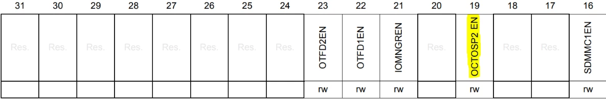
| Dec 2024 | |
| 8.7.28 RCC AHB1 peripheral reset register(RCC_ AHB1RSTR) | Expected: Bit 1 DMA2RST: DMA2 and DMAMUX1 reset | Dec 2024 | ||
| 8.7.30 RCC AHB4 peripheral reset register (RCC_ AHB4RSTR) | Bit 21 BDMARST: BDMA block reset Expected: 0: does not reset the BDMA block (default after reset) | |||
| STM32F303xB/ (Jan 2024) | Figure 14. STM32F303xDxE and STM32F398xE clock tree | Current:  Expected: 
| Mar 2025 | |
| STM32H745/ 755/747/757 RM0399 Rev4 | 9.5 RCC clock block functional description | Current: "USB OTG-FS" Expected: "USB OTG_FS" | Sep 2025 | |
| Figure 60. Kernel clock distribution for DSI and LTDC | Expected: 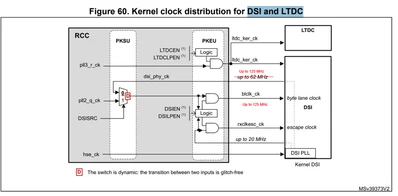
| Mar 2026 | ||
| STM32H503 (Nov 2024) | 10.4.5 PLL description | Current: To ensure an optimal behavior of the PLL when one of the post-divider (DIVP, DIVQ or DIVR) is not used, the application must set the enable bit (DIVyEN) as well as the corresponding post-divider bits (DIVP, DIVQ or DIVR) to 0. Expected: To save power, when the PLLx output (pllx_p_ck, pllx_q_ck or pllx_r_ck) is not used, it should be disabled by clearing the corresponding bit in PLLxCFGR register (PLLxPEN, PLLxQEN or PLLxREN). | Jun 2026 | |
| STM32L41x/42x/ 43x/44x/45x/46x (Dec 2024) | 6.4.26 31 Res. APB2 peripheral clocks enable in Sleep and Stop modes register (RCC_APB2SMENR) | Expected: Reset value: 0x0023 5C01 | Jun 2026 | |
| FLASH | STM32H745/ 755/747/757 (Jun 2023) STM32H742/ 743/753/750 (Jan 2023) STM32H723/ 733/725/735/ 730 (Dec 2021) STM32H7Rx/ RM0477 Rev8 | FLASH erase operations | Current: “1. Check and clear (optional) all the error flags due to previous programming/erase operation. Refer to Section 5.7: FLASH error management for details." Expected: "Remove (optional) word." | Aug 2024
|
| Table xx. Flash interrupt request | Expected: Add notes to Clear flag to resume operation for: -Write protection error: Check this flag after an erase operation. -Programming sequence error and Inconsistency error: Check and clear all the (PGSEER, INCERR, STRBERR) error flags due to previous write operation. | |||
| STM32L4+ (Jun 2021) | Table 9. Flash module - 1 Mbyte single-bank organization, DB1M = 0 (128 bits read width) | Expected: 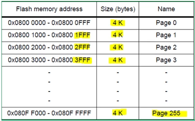
| Sep 2024
| |
| 3.7.8 Flash option register (FLASH_OPTR) | Expected: “Note: For 1-Mbyte and 512-Kbyte Flash memory devices, the DBANK option bit must not be used and must be kept at its ST production value of “1”." | |||
| STM32L0x1 (Feb 2022) | 3.7.8 Option bytes register (FLASH_OPTR) | Expected: RDPROT -> read-only | Mar 2025 | |
| STM32F401xB/ (Jan 2025) | 3.8.5 Flash control register (FLASH_CR) | Bits 6:3 SNB: Sector number Expected: 1100 not allowed | Jun 2025
| |
| STM32F410 (Feb 2025) | ||||
| STM32F412 (Feb 2025) | ||||
| STM32L41x/42x/ 43x/44x/45x/46x (Dec 2024) | 3.4.1 Option bytes description | Current: ST production value: 0xFFEF F8AA Expected: ST production value: 0xFFFF F8AA | ||
| STM32H723/ (Dec 2021) | 4.9.8 FLASH option status register (FLASH_ OPTSR_CUR) | Current: This bit indicates that the product operates below 2.5 V. Expected: 0: I/O speed optimization at low-voltage disabled ( Product working in the full voltage range) | Sep 2025 | |
| 4.9.9 FLASH option status register (FLASH_ OPTSR_PRG) | ||||
| STM32WBA5 (Mar 2025) | Table 40. Flash module 1-Mbyte single bank organization | Current:  Expected: 
| Sep 2025 | |
| STM32G4 (Mar 2025) | Table 5. Boot modes | Current: Main flash memory Expected: Main flash memory bank 1 | Sep 2025 | |
| Forcing boot from user flash memory | Expected: Regardless the boot configuration, it is possible to force booting from a unique entry point in main flash memory bank 1. The BOOT_LOCK option bit must be set. | |||
| Securable memory area Bank 1 option bytes 3.7.17 Flash securable area bank1 register (FLASH_SEC1R) | Bit 16 BOOT_LOCK: used to force boot from user area Expected: 1: Boot forced from main flash memory bank 1 | |||
| STM32H745 RM0399 Rev4 | 4.9.8 FLASH option status register (FLASH_ OPTSR_CUR) | Expected: Remove: "uuuuuuuuuuuuu" | Mar 2026 | |
| STM32H742/ RM0433 Rev8 | ||||
| STM32H723/ (Dec 2021) | 4.4.6 Description of data protection option bytes | Current: RSS can use the full DTCM RAM for executing its services (ST_RAM_SIZE = 11) Expected: RSS can use the DTCM RAM for executing its services (ST_RAM_SIZE). | Mar 2026 | |
| STM32WBA5 (Mar 2025) STM32WBA6 (Dec 2025) | Table XX. User option byte organization mapping | Current: IDWG_SW Expected: IWDG_SW | Mar 2026 | |
| STM32WBA5 (Mar 2025) | 7.9 FLASH registers | Expected: 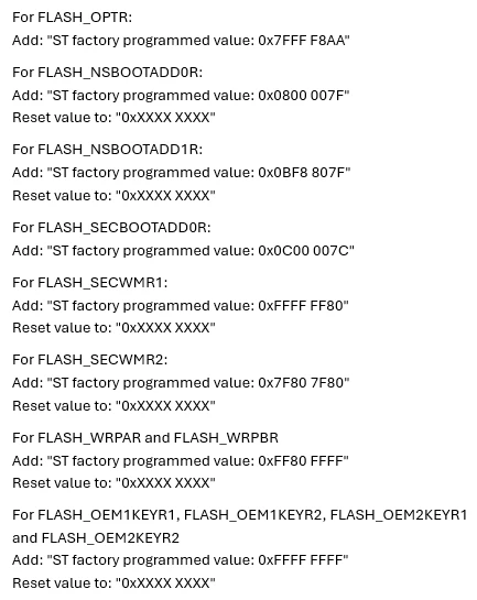
| Mar 2026 | |
| STM32WBA6 (Dec 2025) | 7.9.15 FLASH option register (FLASH_OPTR) | Expected: For FLASH_OPTR: | Mar 2026 | |
| STM32WBA5 (Mar 2025) STM32WBA6 (Dec 2025) | 7.6.2 | Expected: It is easy to move from level 0 or level 0.5 to level 1 by changing the value of the RDP byte to any value (except 0xCC, 0xAA, and 0x55). | Mar 2026 | |
| STM32U0 RM0503 Rev4 | Table 13. Organization of option bytes | Current: Factory value of BOR_EN is 1 Expected: Factory value of BOR_EN is 0 | Mar 2026 | |
| STM32G0x1 (Dec 2024) | Table 17. Organization of option bytes | For address 0x1FFF7838 Expected: FLASH_PCROP2ASR | Jun 2026 | |
| TIM | STM32F469/479 (May 2024) | x.x.x TIM1&TIM8 capture/ | Current: Bits 15:14 Reserved, must be kept at reset value. Expected: Bit 15 CC4NP: Capture/Compare 4 complementary output polarity refer to CC1NP description | Dec 2024 |
| STM32F413/423 (Oct 2024) | ||||
| STM32F410 (Feb 2025) | 14.4.9 TIM1 capture/compare enable register (TIMx_CCER) | Jun 2025 | ||
| STM32H723/ (Dec 2021) | 44.3.11 Combined PWM mode | Expected: When a given channel is used as combined PWM channel, its secondary channel must be configured in the opposite PWM mode (for instance, one in Combined PWM mode 1 and the other in PWM mode 2) | Dec 2024 | |
| STM32U5 (Jan 2025) | 54.3.14 Asymmetric PWM mode | Expected: Figure 549 represents an example of signals that can be generated using asymmetric PWM | Dec 2025 | |
| LPUART | STM32L0x3 (Feb 2022) | Table 150. Error calculation for programmed baud rates at fck = 32 MHz | Expected: Table 150. Error calculation for programmed baud rates at fck = 32.768 KHz | May 2024 |
| RTC | STM32H523/ 533/562/563/573 (Apr 2025) | Table 495. PI8 configuration | Current: Table 495. PI8 configuration Expected: Table 495. PI8/PB2 configuration | Jun 2024 |
| STM32H503 (Nov 2024) | Table 243. RTC register map and reset values (continued) | Expected: RTC_OR register must be removed | Mar 2025 | |
| STM32F405/ (Jun 2024) | Table xxx. RTC register map and reset values | Expected: Add RTC_TSDR register | Jun 2025 | |
| STM32F469/479 (May 2024) | ||||
| STM32F410 (Feb 2025) | ||||
| STM32F412 (Feb 2025) | ||||
| STM32F413/423 (Oct 2024) | ||||
| STM32F401xB/ C/D/E (Jan 2025) | Table 68. RTC register map and reset values | Add: - RTC_TSDR register - RTC_SHIFTR register | Jun 2025 | |
| STM32H745/ 755/747/757 RM0399 Rev4 | x.x.x RTC block diagram | Expected: – Tamper detection erases immediately the backup registers. The backup SRAM is read-protected after a tamper detection, and software can launch its mass erase by writing a dummy zero data to the backup SRAM. | Sep 2025 | |
| STM32H723/ RM0468 Rev3 | ||||
| STM32H742/ (Jan 2023) | ||||
|
(Dec 2021) | 51.4.15 Tamper detection | Current: RTC_TAMPCR Expected: RTC_TAFCR | Mar 2026 | |
| ETH | STM32H723/ (Dec 2021) | Table xxx. Ethernet peripheral pins | Expected: Remove "ETH_PHY_INTN" from Table Ethernet peripheral pins | Apr 2024 |
| STM32H742/ (Jan 2023) | May 2024 | |||
| STM32H523/ 533/562/563/573 (Apr 2025) | 57 Ethernet (ETH): media access control | Expected: 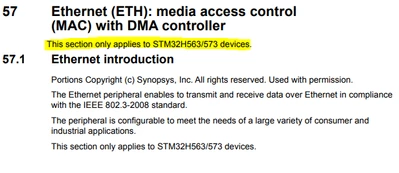
| Sep 2024 | |
| PWR | STM32F76x/77x (Jul 2024) | 4.3 Low-power modes | Expected: "The MCU exits from Standby low-power mode through an external reset (NRST pin), an IWDG reset, a rising or falling on one of the enabled WKUPx pins or a RTC event occurs" | Aug 2024 |
| STM32L41x/42x/ | 4.4 PWR registers | Expected: This register is neither reset when exiting Standby mode, nor by the PWRRST bit in the RCC_APB1RSTR1 register. | ||
| Jun 2025 | ||||
|
| ||||
| STM32L41x/42x/ | 5.3.9 Standby mode | Expected: The SBF status flag in the Power status register (PWR_SR1) | Mar 2025 | |
| STM32U0 RM0503 Rev4 | 4.1.4 Battery backup domain | Current: PA0/RTC_TAMP2 and PE6/RTC_TAMP3 when they are configured by the RTC as tamper pins. Expected: TAMPER pins, when configured to the tamper role, see datasheet for list of pins available for tamper feature. | Sep 2025 | |
| STM32F405/ RM0090 Rev21 | 5.1.3 Voltage regulator for STM32F405xx | Scale 1 or scale 2 can be configured on the fly through VOS Current: (bit 15 of the PWR_CR register). Expected: (bit 14 of the PWR_CR register). | Mar 2026 | |
| STM32H745/ 755/747/757 RM0399 Rev4 | Figure 28. DSI supply configuration | Expected: Remove "DSI PHY external supply" Figure | Mar 2026 | |
| COMP | STM32F303xB/ (Jan 2024) | 17.5 COMP registers | Current: Expected: 00: High speed | Apr 2024 |
| Table 109. COMP register map and reset values | Current: 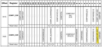 Expected: 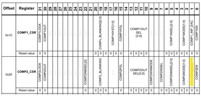
| Mar 2026 | ||
| STM32L41x/42x/ (Dec 2024) | Figure 118. Comparator block diagram | Current: STM32L45xxx and STM32L46xxx devices feature only DAC_CH1 Expected: On devices with single DAC there is a single DAC input" instead of existing | Jun 2026 | |
| 19.6.1 Comparator 1 control and status register (COMP1_CSR) | Current: 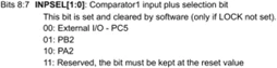  Expected: 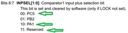 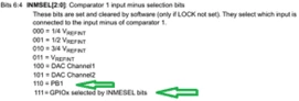
| Jun 2026 | ||
| STM32G4 (Mar 2025) | Table 201. Blanking sources | Expected: A new row must be added for value "000" for "disabled" for all COMPs (COMP1 to COMP7) | Jun 2026 | |
| STM32G0x1 (Dec 2024) | 18.5 COMP interrupts | Expected: 
| Jun 2026 | |
| DBG | STM32U5 (Jan 2025) | 75.8.1 BPU registers | Bit 1 KEY: Write protect key Current: Expected: A write to BPU_CTRLR register is ignored if this bit is not set to 1. | Oct 2024 |
| GPIO | STM32L47x/ 48x/49x/4Ax (Oct 2023) | 8.4 GPIO functional description | Add: 
| Oct 2024 |
| 8.2 GPIO main features | Add: Configurable state of each I/O in Standby mode: floating, pull-up/down, analog. | Oct 2024 | ||
| STM32H723/ RM0468 Rev3 | 11.3.11 I/O compensation cell | Add: 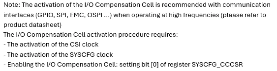
| Mar 2025 | |
| STM32H742/ (Jan 2023) | 11.4.10 GPIO alternate function high register (GPIOx_AFRH) (x = A to J) | Current: Address offset: 0x2. Expected: Address offset: 0x4 | Sep 2025 | |
| STM32H745/ 755/747/757 RM0399 Rev4 | Figure 76. Basic structure of an I/O port bit Figure 77. Basic structure of a 5-Volt tolerant I/O port bit | Expected: The protection diodes connected to VDD and VDD_FT removed. Change the label on diodes to VSS FROM "Protection | Dec 2025 | |
| STM32L41x/42x/ (Dec 2024) | 8.5.3 GPIO port output speed register (GPIOx_OSPEEDR) (x = A to E, H) | 8.5.3 GPIO port output speed register (GPIOx_OSPEEDR) (x = A to E, H) | Jun 2026 | |
| DMA | STM32L47x/ 48x/49x/4Ax (Oct 2023) | Table 43. DMA1 and DMA2 implementation | Current: 1. HASH related DMA channel is only applicable for STM32L4Ax devices. Expected: 1. HASH related DMA channel is only applicable for STM32L4Ax/L49x devices. | Oct 2024 |
| Table 45. DMA2 requests for each channel Figure 31. DMA block diagram | Expected: "3. Only available on STM32L4Ax/L49x devices." | Oct 2024 | ||
| Memory and bus architec- ture | STM32H745/ 755/747/757 (Jun 2023) STM32H742/ (Jan 2023) STM32H723/ (Dec 2021) | AXI interconnect - INI x AHB functionality modification register | Expected: Bit 1 WR_INC_OVERRIDE: Converts all AHB-Lite write transactions to a series of single beat AXI transactions, and each AHB-Lite write beat is acknowledged with the AXI buffered write response. Bit 0 RD_INC_OVERRIDE: Converts all AHB-Lite read transactions to a series of single beat AXI transactions. | Jul 2024 |
| STM32H723/ (Dec 2021) | Table 7. Register boundary addresses | Expected: Add: | Dec 2024 | |
| STM32F303xB/ (Jan 2024) | Figure 1. STM32F303xB/C and STM32F358xC system architecture Figure 2. STM32F303x6/8 and STM32F328x8 system architecture Figure 3. STM32F303xDxE and STM32F398xE system architecture | Current: FLTIF Expected: FLITF | Mar 2025 | |
| STM32F446 RM0390 Rev7 | Figure 2. Memory map | Expected: 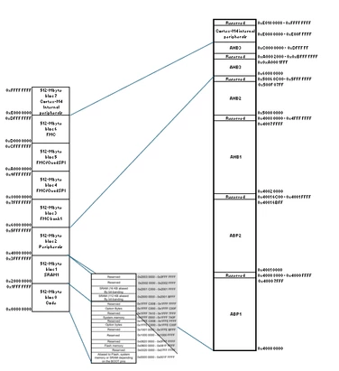
| Mar 2026 | |
| STM32U0 (Jul 2025) | 2.5 Boot configuration | Remove: 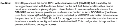
| Mar 2026 | |
| LCD | STM32U0 (Jul 2025) | 19 Liquid crystal display controller (LCD) | Add: 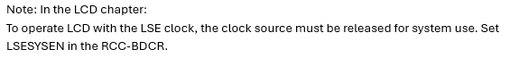
| Nov 2024 |
| OCTOSPI | STM32L552/562 (Jun 2025)
| 20.4.15 OCTOSPI Regular-command mode configuration | Current: This shift is performed by an external delay block located outside the OCTOSPI. The control of this feature depends on the device implementation (see the product reference manual for more details). Expected: This shift is controlled via the RCC_DLYCFGR register. | Dec 2024 |
| 20.7.2 OCTOSPI device configuration register 1 (OCTOSPI_ | Expected: | |||
| Device electronic signature | STM32H723/ (Dec 2021) | 66.4 Package data register | Add: 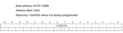
| Mar 2025 |
| STM32G0x1 (Dec 2024) | 41.1 Unique device ID register (96 bits) | Expected: Bits 31:0 UID [31:0]: X and Y coordinates on the wafer | Jun 2026 | |
| SYSCFG | STM32H723/ (Dec 2021)
| 12.4.7 SYSCFG compensation cell control/status register | Current: It must be used only if the product supply voltage is below 2.5 V. Setting this bit when VDD is higher than 2.5 V might be destructive. Expected: It must be used in the product supply voltage conditions described in product datasheet. | Sep 2025 |
| 12.4.25 SYSCFG user register 17 (SYSCFG_UR17) | Current: Expected: It must be used in the product supply voltage conditions described in product datasheet. | Sep 2025 | ||
| TAMP | STM32H503 (Nov 2024) | 33.6.16 TAMP option register (TAMP_OR) | Add section: 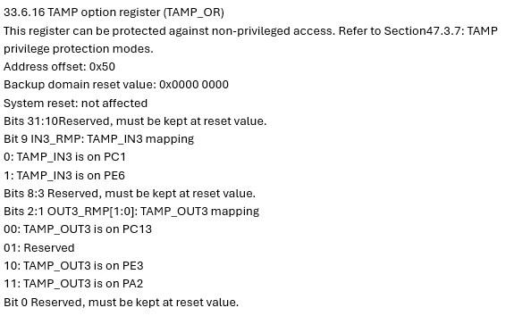
| Mar 2025 |
| System security | STM32H523/ 533/562/563/573 (Apr 2025) | Table 20. Main product life cycle transitions | Add: 
| Mar 2025 |
| STM32H503 (Nov 2024) | Table 5. Main product life-cycle transitions | |||
| SPI | STM32F401xB/C/ (Jan 2025) | Table 93. SPI register map and reset values | Add: SPI_CR2 register | Jun 2025 |
| STM32F446 RM0390 Rev7 | 26.3.2 Communications between one master and one slave | Expected: The SPI can communicate in simplex mode by setting the SPI in transmit-only or in receive-only using the RXONLY bit in the SPIx_CR1 register. | Dec 2025 | |
| ADC | STM32H723/ (Dec 2021) | Figure 162. ADC1 connectivity | Current: -ADC1_INP14 -ADC1_INP15 -ADC1_INP16 -ADC1_INP17 -ADC1_INP18 -ADC1_INP19 Expected: -ADC12_INP14 -ADC12_INP15 -ADC12_INP16 -ADC12_INP17 -ADC12_INP18 -ADC12_INP19 | Jun 2025 |
| STM32H723/ (Dec 2021) | 28.7.2 ADC common control register (ADCx_CCR) (x=1/2) | Current: adc_ker_ck= 2 x adc_hclk. Expected: adc_sclk = 2 x adc_hclk | Sep 2025 | |
| STM32H742/ (Jan 2023) | 25.7.2 ADC x common control register (ADCx_CCR) (x=1/2 or 3) | |||
| STM32H745/ 755/747/757 RM0399 Rev4 | x | Current: legacy Expected: standard | Mar 2026 | |
| STM32H723/ (Dec 2021) | 28 | |||
| STM32U0 RM0503 Rev4 | 14.4.8 Channel selection (CHSEL, SCANDIR, CHSELRMOD) | Remove: When VREF+ is lower than VDDA, this channel is not converted. | Mar 2026 | |
| STM32G4 (Mar 2025) | Managing conversions using the DMA | Current: 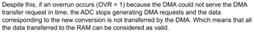 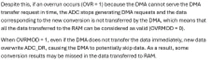
| Jun 2026 | |
| FMC | STM32F446 RM0390 Rev7 | SDRAM control register x (FMC_SDCRx) | Current: Expected: HCLK | Sep 2025 |
| System and memory overview | STM32L41x/42x/ RM0394 Rev5 | Table 2. STM32L41xxx/ | Current: TAMP(3) 3. Not available on STM32L41xxx and STM32L42xxx devices Expected: TAMP(9) 9. Available on STM32L41xxx and STM32L42xxx devices only. | Sep 2025 |
| STM32L47x/ 48x/49x/4Ax (Oct 2023) | Figure 1. System architecture for STM32L47x/L48x devices | Expected: SRAM2 and S-bus must be connected. | Dec 2025 | |
| STM32L41x/42x/ (Dec 2024) | Figure 1. System architecture | |||
| USB | STM32H745/ 755/747/757 RM0399 Rev4 | 60.7.2 USB host states | Expected: 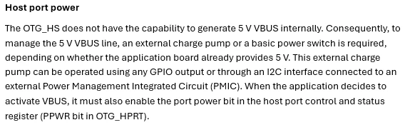
| Sep 2025 |
| STM32H723/733/ (Dec 2021) | Table 542. OTG_HS register map and reset values | Current: At offset 0x120 -> OTG_DIEPTXF7 Expected: At offset 0x120 -> OTG_DIEPTXF8 | Sep 2025 | |
| SMM | STM32H723/733/ (Dec 2021) | 5.4 Root secure services (RSS) | Add: The root secure services (RSS) are STMicroelectronics ROM code stored on the device. 
| Sep 2025 |
| STM32H745/ 755/747/757 RM0399 Rev4 STM32H742/ RM0433 Rev8 | 5.4 Root secure services (RSS) 5.4.1 Secure area setting service | Add: 
|
Mar 2026 | |
| Current:  Expected: 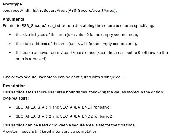
| ||||
| FDCAN | STM32H503 (Nov 2024) | 39.3.3 Bit timing | Current: A valid edge is defined as the first transition in a bit time from dominant to recessive bus level, Expected: A valid edge is defined as the first transition in a bit time from recessive to dominant bus level, | Dec 2025 |
| STM32G4 (Mar 2025) | 4.4.18 FDCAN interrupt line enable register(FDCAN | Expected: Bit 1 EINT1: Enable interrupt line 1 | Mar 2026 | |
| Memory and bus architec-ture | STM32H742/ RM0433 Rev8 | Table 3. Bus-master-to-bus-slave interconnect | Expected: The 'x' from the circled boxes are removed 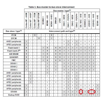 | Dec 2025 |
| I2S | STM32F446 (Feb 2026) | Section 27 “Inter-integrated circuit (I2C) interface |
"ITEVFEN" Expected: "ITEVTEN" | Mar 2026 |
| HRTIM | STM32G4 (Mar 2025) | 28.5.x HRTIM ADC trigger x register (HRTIM_ADCxR) | Expected: - Bit 22 ADC2TCRST: ADC trigger 2 on timer C reset and counter roll-over(1) -Bit 22 ADC4TCRST: ADC trigger 4 on timer C reset and counter roll-over(1) | Mar 2026 |
| Radio system | STM32WBA5 (Mar 2025) | Table 78. 2.4 GHz RADIO supply configuration | Current: Expected: 2.1 V | Mar 2026 |
| LPTIM | STM32U0 RM0503 Rev4 | Table 153. LPTIM1/3 input capture 2 connections | Current: Expected: Table 153. LPTIM1/3 input capture 3 connections | Mar 2026 |
| Table 154. LPTIM1/2/3 input capture 2 connections | Current: Expected: Table 154. LPTIM1/3 input capture 4 connections |