STM32 MCU errata sheets: Expected preliminary updates
- June 6, 2024
- 0 replies
- 4840 views
Introduction
This article includes preliminary updates of STM32 MCU errata sheets reported since 1st January 2024. It highlights the current description requiring update and the expected one if available.
The purpose of this article is to deliver any expected updates to our MCU errata sheets prior to actual documentation releases. We wish to be transparent with our updates and provide them as fast as possible, to assist you in your design process.
This article is updated on a quarterly basis. Once these preliminary updates are manifested in the errata sheets, this article is refreshed with new information.
Moving forward, we are also working on providing errata sheet releases on a more frequent basis.
IMPORTANT NOTICE - READ CAREFULLY:
- STMicroelectronics NV and its subsidiaries (“ST”) reserve the right to make changes, corrections, enhancements, modifications, and improvements to this article at any time without notice.
- Information in this article supersedes and replaces information previously supplied in any prior versions of this article.
- The following table gives a quick reference to the preliminary documentation updates which may be changed or improved without notice.
- This article will be reviewed on a quarterly basis and applied updates will be removed from the table.
- The hyperlinks under "Doc Reference - Revision" provides a direct link to the specific document page where the description is located.
Summary of documentation updates: "STM32 MCU errata sheets"
| Function | Series/Lines | Doc Reference - Revision | Description | Date of added update |
| SPI | STM32F427xx STM32F437xx STM32F429xx STM32F439xx | (Feb 2025) | Add section: Corrupted last bit of data and/or CRC, received in Master mode with delayed SCK feedback Description Workaround 
| Mar 2024
|
| System | STM32G471xx | (Jun 2024) | Remove section: The same errata looks to appear 2 times : 2.2.5 MCU cannot enter in Standby mode when HSE bypass used | Jun 2025 |
| IWDG | STM32F100x4 STM32F100x6 | (Jul 2022) | Remove sections: Delete duplicated sections: - RVU flag not cleared at low APB clock frequency - PVU flag not cleared at low APB clock frequency | Mar |
| STM32F10xx4 STM32F10xx6 | (Jun 2022) | |||
| STM32F101xF | (Jul 2022) | |||
| STM32F101xC | (Jun 2022) | |||
| STM32F105xx STM32F107xx | (Jun 2022) | |||
| STM32F100xC STM32F100xD STM32F100xE | (Aug 2022) | |||
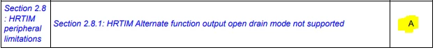
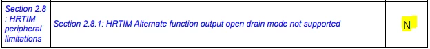
| HRTIM | STM32F334x4 | (Aug 2021) | Table 4. Summary of silicon limitations Current:
A = limitation present, workaround available Expected: With N = limitation present, no workaround available | Nov 2024 |
| ADC | STM32L412xx | ES0456 Rev6 (Nov 2024) | Remove section: Delete duplicated section: "2.6.9 Writing ADCx_JSQR when JADCSTART and JQDIS are set might lead to incorrect behavior" should be removed. It is duplicated with "2.6.1 Writing ADC_JSQR when JADCSTART and JQDIS are set may lead to incorrect behavior" | Dec 2024 |
| STM32G491xx STM32G4A1xx | (Jun 2024) | Update section: 2.5.11 An ADC instance may impact the accuracy of another ADC instance at specific conditions Expected: 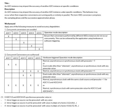
| Jun 2026 | |
| STM32G431xx STM32G441xx | (Jun 2024) | |||
| STM32G471xx STM32G473xx STM32G474xx STM32G483xx STM32G484xx | (Jun 2024) | Update section: 2.7.11 An ADC instance may impact the accuracy of another ADC instance at specific conditions Expected: 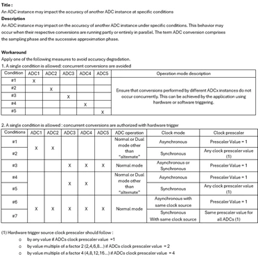
| Jun 2026 | |
| CEC | STM32H7A3xI STM32H7A3xG | ES0478 Rev11 (Apr 2022) | Add section: Unexpected TXERR flag during a message transmission. Description During the transmission of a 0 or a 1, the HDMI-CEC drives the open-drain output to high-Z, so that the external pull-up implements a voltage rising ramp on the CEC line. | Dec 2024 |
| OCTOSPI | STM32H7A3xI STM32H7A3xG | ES0478 Rev11 (Apr 2022) | Add section: Transactions are limited to 8 Mbytes in OctaRAM™ memories. Description When the controller is configured in Macronix OctaRAM™ mode, by setting the MTYP[2:0] bitfield of the OCTOSPI_DCR1 register to 011, only 13 bits of row address are decoded and sent to the memory, meaning that only 8 K of 1-Kbyte blocks can be accessed (8 Mbytes). | Dec 2024 |
| Applicability | STM32H7A3xI STM32H7A3xG STM32H7B0xB STM32H7B3xI | (Apr 2022) | Table 1. Device summary Add: STM32H7A3LG in the part numbers list. | Jun 2025 |
| STM32U375xx STM32U385xx | (Jan 2026) | Current: 2. REV_ID[5:0] bitfield of DBGMCU_IDCODE fuse Expected: 2. REV_ID[15:0] bitfield of DBGMCU_IDCODE fuse | Dec 2025 | |
| TIM | STM32F105xx STM32F107xx | (Jun 2022) | Remove section: Delete duplicated sections - PWM re-enabled in automatic output enable mode despite of system break - TRGO and TRGO2 trigger output failure - Consecutive compare event missed in specific conditions - Output compare clear not working with external counter reset | Jun 2026 |
| STM32F10xx4 STM32F10xx6 | (Jun 2022) | |||
| Summary of device errata | STM32F058C8 STM32F058R8 | (Oct 2020) | Add in Table 2. Summary of device limitations: 2.2.1 Wakeup sequence from Standby mode when using more than one wakeup source | Jun 2026 |
| USART | STM32WLE5xx STM32WLE4xx | (Mar 2023) | Add in Table 2. Summary of device limitations: 2.8.2 Data corruption due to noisy receive line | Jun 2026 |