- STMicroelectronics Community
- Knowledge base
- STM32 MCUs
- How to correctly setup your application to use USB...
- Subscribe to RSS Feed
- Mark as New
- Mark as Read
- Bookmark
- Subscribe
- Email to a Friend
- Printer Friendly Page
- Report Inappropriate Content
How to correctly setup your application to use USB DMA controller with STM32H7 devices
- Subscribe to RSS Feed
- Mark as New
- Mark as Read
- Bookmark
- Subscribe
- Email to a Friend
- Printer Friendly Page
- Report Inappropriate Content
on
2021-03-26
12:38 PM
- edited on
2024-06-04
06:03 AM
by
![]() Laurids_PETERSE
Laurids_PETERSE
Introduction
This FAQ concerns enabling USB DMA in STM32H7 devices. Many customers that are working with USB in STM32H7 devices face a problem when activating DMA. What they notice is that everything is working good and USB behaves normally before activating DMA. Once they enable DMA, everything falls down, and this is common for both USB host and device:
hpcd.Init.dma_enable = ENABLE;
or
hhcd.Init.dma_enable = ENABLE;
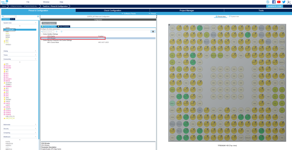
This problem is related to two possible root causes: memory layout on STM32H7 and internal data cache (D-Cache) of the Cortex-M7 core. This will be explained with more details later.
In summary these can be the possible issues:
- Variables and buffers are placed in DTCM SRAM. Unfortunately, DTCM SRAM is set as default memory location in some projects including examples.
- D-Cache enabled for DMA buffers, different content in cache and in SRAM memory (Data coherency issue)
- Starting the DMA just after writing the data to TX buffer, without synchronization barriers (placing __DSB() instruction between last data write and DMA enable).
1. Possible root cause 1: STM32H7 memory layout
STM32H7 devices contain basically three domains D1, D2, and D3. However, in some devices (STM32H7A3/7B3 and STM32H7B0), we can find only two domains, where D1 and D2 domains are merged into one domain which is the CD Domain, and D3 is nominated as SRD Domain.
In this FAQ, we will study the case of STM32H7 devices with three domains. But this can be applicable for all other STM32H7 devices when taking in consideration the alignments previously explained.
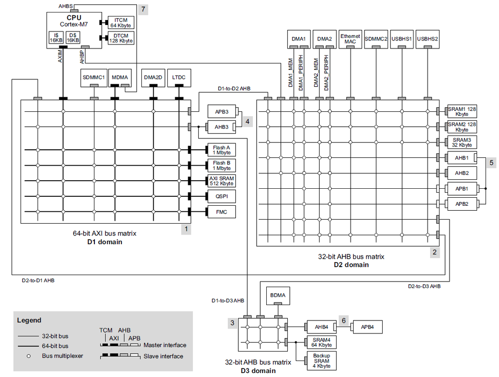
As we previously explained, most of STM32H7 devices consist of three bus matrix domains (D1, D2, and D3) as seen on the picture below.
D1 and D2 domains are connected through bus bridges, both can also access data in D3 domain. However, there is no connection from D3 domain to D1 or D2 domain.
The DMA1 and DMA2 controllers are located in D2 domain and can access almost all memories with exception of ITCM and DTCM RAM (located at 0x20000000). This DMA is used in most cases.
BDMA controller is located in D3 domain and can access only SRAM4 and backup SRAM in D3 domain.
MDMA controller is located in D1 domain and can access all memories, including ITCM/DTCM. This controller is mainly used for handling D1 peripherals and memory transfers between domains.
In the previous figure, we can see that USBHS1 and USBHS2 are located in D2 domain and have no interconnection with DTCM RAM which is the default memory used in approximately all USB projects. Therefore when enabling the internal DMA USB, projects do not work, as DMA will not be able to access the data buffers placed in DTCM and it results in DMA transfer error.
2. Possible root cause 2: Handling DMA buffers with D-Cache enabled
The Cortex-M7 contains two internal caches, I-Cache for loading instructions and D-cache for data. The D-Cache can affect the functionality of DMA USB transfers, since the default cache policy for product SRAMs is normal memory (cacheable). Cache will hold the new data in the internal cache and don't write them to SRAM memory. However, the DMA controller loads the data from SRAM memory and not D-Cache. Same behavior can happen when reading data, as USB DMA will update buffers in SRAM, and the content of SRAM will not be immediately visible to CPU as CPU will see previously cached data. This will result in data coherency issues.
There are several ways how to keep manage USB DMA with D-cache:
-
Use cache maintenance operations: before enabling DMA, the software can request a cache clean operation to write data to SRAM, and before reading, the software can request to clean and invalidate cache to re-synchronize with the new SRAM content.
-
Disable D-Cache for part of the memory: use MPU to change DMA buffers to non-cacheable (device mode)
-
Disable D-Cache globally: but this might result in performance loss, and it is not recommended.
3. Solution: Example with STM32H743I-EVAL, STM32CubeMX, & STM32CubeIDE
To synthetize what explained previously, we represent in this section an example that uses STM32H743I-EVAL board, but this is applicable for all STM32H7 devices.
-
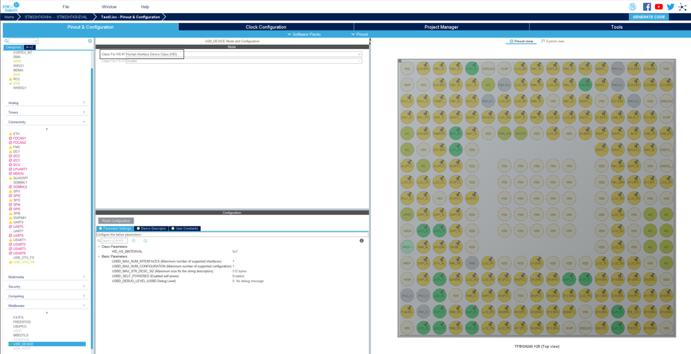
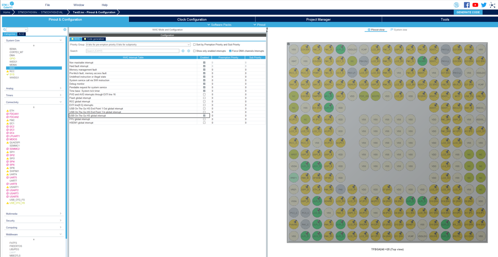
Project Creation & Generation: In this section, we will create and generate the USB project using STM32CubeMX. We will take as example the Human Interface Device Class (HID) USB HS application, but this is applicable for all other USB Device and Host projects. The following figure shows the configuration that should be set:
After generating the project with your preferable tool (we are using IAR in this tutorial), you can see that the HID application runs perfectly and the HID-compliant mouse is well detected through Device Manager.
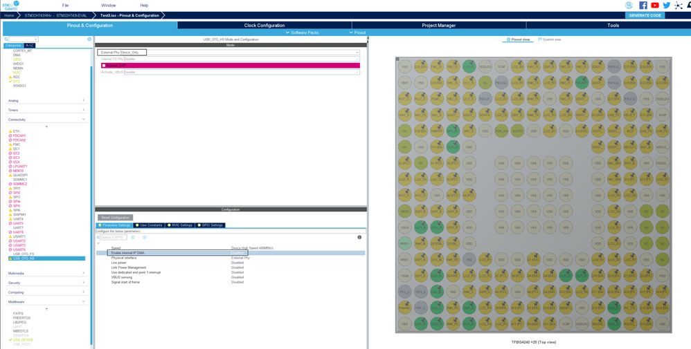
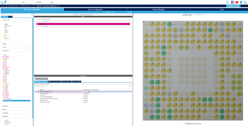
Now, we will enable DMA IP:
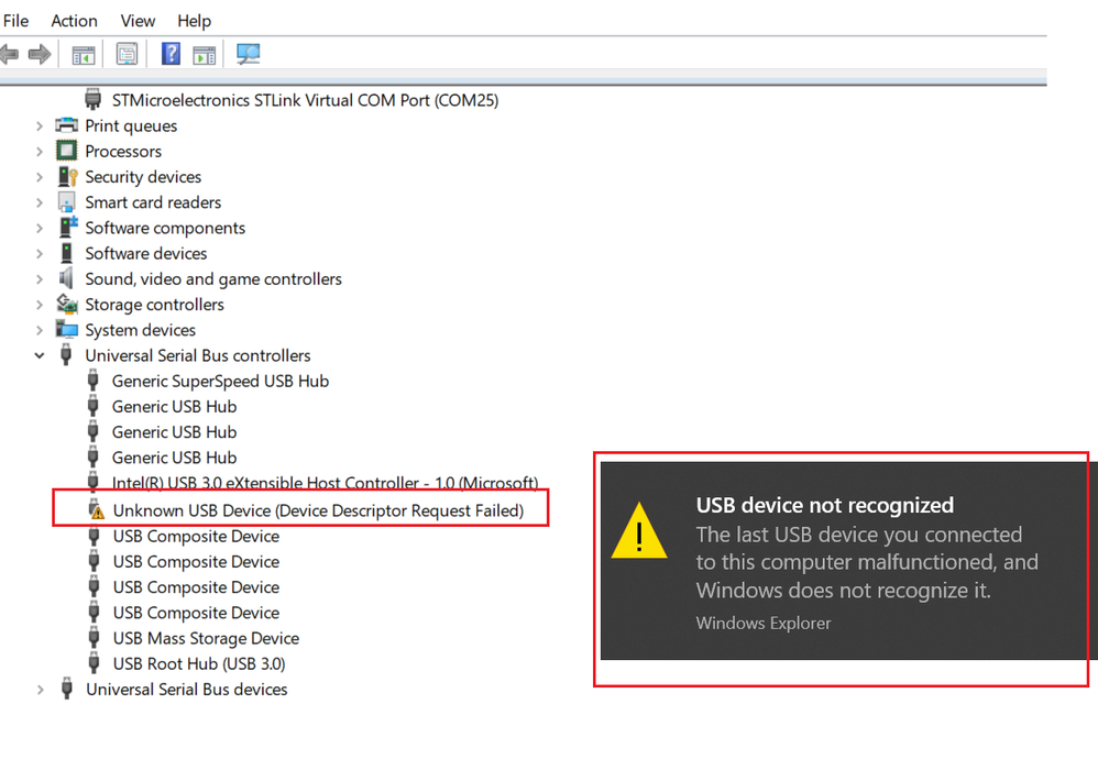
After generating the project, you can remark that enumeration is lost and your laptop cannot detect HID device properly anymore.
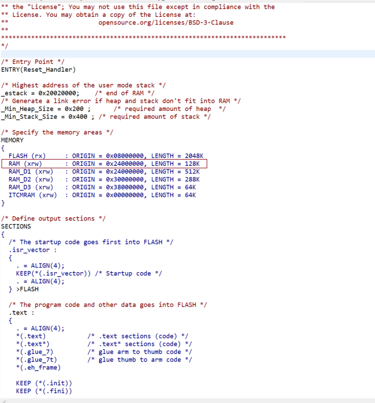
The default memory allocation generated by STM32CubeMx and used by most of USB application in the STM32CubeH7 Firmware package is DTCM, which is not accessible by USB. After referencing to the corresponding reference manual, you can find memories accessible by USB under System Architecture section. So let change the DTCM memory with another one which is accessible by USB, for example AXI SRAM 0x2400 0000.
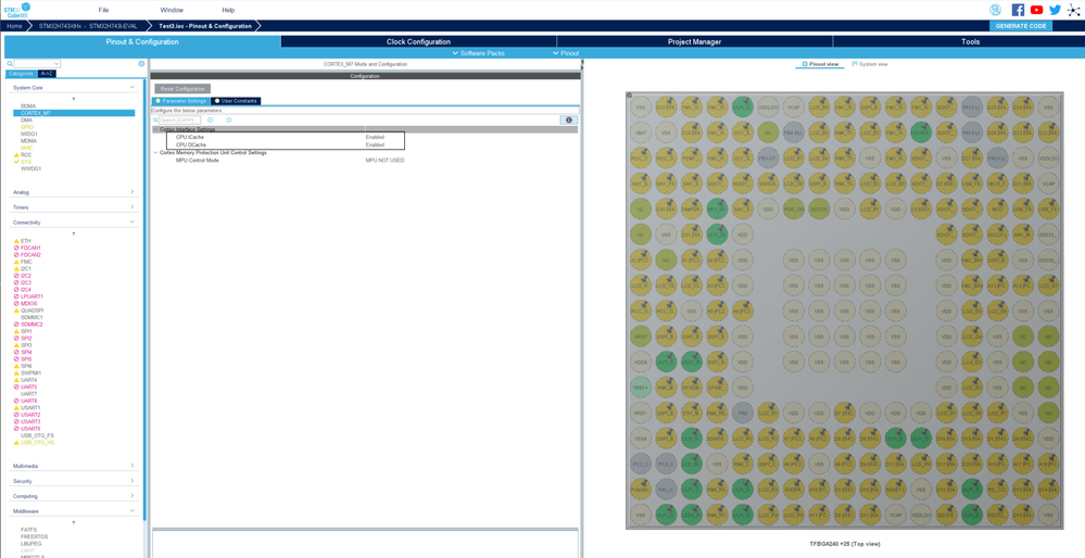
Unfortunately, this configuration is not enough, but for the purpose of the example we will apply the simpler solution to confirm that the issue is related to data coherency. We will disable the data cache as explained previously.
Now, you can see your HID-compliant mouse device is well enumerated by Device Manager.
4. References:
- FAQ: DMA is not working on STM32H7 devices
- AN4838: Managing memory protection unit (MPU) in STM32 MCUs
- AN4839: Level 1 cache on STM32F7 Series and STM32H7 Series
- AN4891: STM32H7x3 system architecture and performance software expansion for STM32Cube
- Mark as Read
- Mark as New
- Bookmark
- Permalink
- Email to a Friend
- Report Inappropriate Content
Great explanation!!!
- Mark as Read
- Mark as New
- Bookmark
- Permalink
- Email to a Friend
- Report Inappropriate Content
Thanks. Quite good explanation!
Really it start working when D-Cache disabled and all data placed in AXI_SRAM.
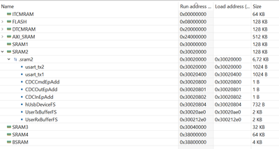
But what need change if I want place all input and output buffers in SRAM2 region ?
program payload buffers not a question, means all what need related to USB_CDC DMA data?
By manual SRAM2 closer to USB than AXI_SRAM. I can send data using massive placed at SRAM2 and USB HAL data at AXI_RAM. but once I enable D-Cache, catch Hard_fault. USB completely no init.
( SRAM2 (rw) : ORIGIN = 0x30020000, LENGTH = 128K)
trying one by one place HAL USB_CDC components to SRAM2 from AXI_SRAM, useless :(
- Mark as Read
- Mark as New
- Bookmark
- Permalink
- Email to a Friend
- Report Inappropriate Content
Hi @AGord.2
I recommend creating a new post on STM32 MCUs products - STMicroelectronics Community to get assistance.
