- STMicroelectronics Community
- Knowledge base
- STM32 MCUs
- How to avoid a HardFault when ICACHE is enabled on...
- Subscribe to RSS Feed
- Mark as New
- Mark as Read
- Bookmark
- Subscribe
- Email to a Friend
- Printer Friendly Page
- Report Inappropriate Content
How to avoid a HardFault when ICACHE is enabled on the STM32H5 series
- Subscribe to RSS Feed
- Mark as New
- Mark as Read
- Bookmark
- Subscribe
- Email to a Friend
- Printer Friendly Page
- Report Inappropriate Content
on
2024-01-19
6:35 AM
- edited on
2025-11-26
5:51 AM
by
![]() Laurids_PETERSE
Laurids_PETERSE
Introduction
This article presents a quick guidance on how to prevent HardFault occurrences when the ICACHE is enabled on the STM32H5 MCU.
1. Summary and description
This article explains why a HardFault may occur when accessing the following:
- Internal reference voltage (VREFINT)
- Internal temperature sensor (VSENSE)
- Unique device ID
- Package ID data
- How the CACHE intervenes in accessing data on the STM32H5 series.
2. Root cause
The internal reference voltage (VREFINT), the internal temperature sensor (VSENSE), the unique device ID, and the package ID data are located in RO and OTP areas.
By default, all the AHB memory range is cacheable. For OTP and RO regions, caching is not practical and MPU has to be used to disable local cacheability.
3. RO and OTP areas
The embedded flash memory offers a 2-Kbyte memory area to store read-only data. This area is mapped as described in the below table:
* VREFINT_CAL_ADR, TEMPSENSOR_CAL1_ADDR, and TEMPSENSOR_CAL2_ADDR are located in reserved information
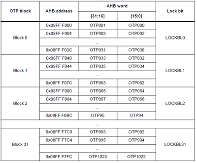
OTP data is organized as 32 blocks of 32 OTP words, as shown in the below table:
It is also important to note that for 8-bit accesses, an AHB bus error is generated. For OTP and RO sectors in memory, a 6-bit ECC code is associated with each 16-bit data flash word. So, the embedded flash memory supports only16-bit or 32-bit write operations. Therefore, the burst access is not supported for these regions.
4. MPU configuration
You can refer to the following MPU configuration to disable cacheability for OTP and RO regions
#include "stm32h5xx_hal.h"
void MPU_Config(void);
/* MPU attribute setting */
#define DEVICE_nGnRnE 0x0U /* Device, noGather, noReorder, noEarly acknowledge. */
#define DEVICE_nGnRE 0x4U /* Device, noGather, noReorder, Early acknowledge. */
#define DEVICE_nGRE 0x8U /* Device, noGather, Reorder, Early acknowledge. */
#define DEVICE_GRE 0xCU /* Device, Gather, Reorder, Early acknowledge. */
#define WRITE_THROUGH 0x0U /* Normal memory, write-through. */
#define NOT_CACHEABLE 0x4U /* Normal memory, non-cacheable. */
#define WRITE_BACK 0x4U /* Normal memory, write-back. */
#define TRANSIENT 0x0U /* Normal memory, transient. */
#define NON_TRANSIENT 0x8U /* Normal memory, non-transient. */
#define NO_ALLOCATE 0x0U /* Normal memory, no allocate. */
#define W_ALLOCATE 0x1U /* Normal memory, write allocate. */
#define R_ALLOCATE 0x2U /* Normal memory, read allocate. */
#define RW_ALLOCATE 0x3U /* Normal memory, read/write allocate. */
#define OUTER(__ATTR__) ((__ATTR__) << 4U)
#define INNER_OUTER(__ATTR__) ((__ATTR__) | ((__ATTR__) << 4U))
/**
* @brief Configure the MPU attributes.
* @note The Base Address is RO area
* None
* @retval None
*/
void MPU_Config(void)
{
MPU_Attributes_InitTypeDef attr;
MPU_Region_InitTypeDef region;
/* Disable MPU before perloading and config update */
HAL_MPU_Disable();
/* Define cacheable memory via MPU */
attr.Number = MPU_ATTRIBUTES_NUMBER0;
attr.Attributes = INNER_OUTER(NOT_CACHEABLE);
HAL_MPU_ConfigMemoryAttributes(&attr);
/* BaseAddress-LimitAddress configuration */
region.Enable = MPU_REGION_ENABLE;
region.Number = MPU_REGION_NUMBER0;
region.AttributesIndex = MPU_ATTRIBUTES_NUMBER0;
region.BaseAddress = 0x08FFF800;
region.LimitAddress = 0x08FFFFFF;
region.AccessPermission = MPU_REGION_ALL_RW;
region.DisableExec = MPU_INSTRUCTION_ACCESS_DISABLE;
region.IsShareable = MPU_ACCESS_NOT_SHAREABLE;
HAL_MPU_ConfigRegion(®ion);
/* Enable the MPU */
HAL_MPU_Enable(MPU_PRIVILEGED_DEFAULT);
}
void MX_ICACHE_Init(void)
{
/* USER CODE BEGIN ICACHE_Init 0 */
/* USER CODE END ICACHE_Init 0 */
/* USER CODE BEGIN ICACHE_Init 1 */
/* USER CODE END ICACHE_Init 1 */
/** Enable instruction cache in 1-way (direct mapped cache)
*/
if (HAL_ICACHE_ConfigAssociativityMode(ICACHE_1WAY) != HAL_OK)
{
Error_Handler();
}
if (HAL_ICACHE_Enable() != HAL_OK)
{
Error_Handler();
}
/* USER CODE BEGIN ICACHE_Init 2 */
/* USER CODE END ICACHE_Init 2 */
}
5. How does the cache intervene in access to data in the STM32H5 series?
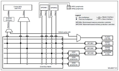
The STM32H503xx microcontrollers features an integrated ICACHE that combines instructions and data into a single cache. This cache is introduced on the C-AHB code bus of the Cortex®-M33 processor. This is to improve performance when fetching instructions (or data) from internal memories (SRAM1 and SRAM2).
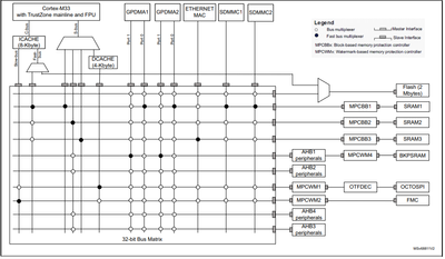
The STM32H562xx, STM32H563xx, and STM32H573xx microcontrollers features:
- A DCACHE S-bus that connects the system bus of the Cortex®-M33 core to the BusMatrix via the data cache. This bus targets the external memories (FMC and OCTOSPI)
- An ICache that is connected via the fast C-bus to the internal flash memory and the internal SRAMs (SRAM1, SRAM2 and SRAM3), and it is connected via the slow bus to the external memories (FMC and OCTOSPI)
Related links
- Mark as Read
- Mark as New
- Bookmark
- Permalink
- Email to a Friend
- Report Inappropriate Content
Using the term "ICACHE" for this was a quintessentially horrible idea. Thanks for the permanent confusion!
- Mark as Read
- Mark as New
- Bookmark
- Permalink
- Email to a Friend
- Report Inappropriate Content
Going to back link to failure examples to help search/index
- Mark as Read
- Mark as New
- Bookmark
- Permalink
- Email to a Friend
- Report Inappropriate Content
I've read this 3 times back and forth but still cannot understand ((
So, does the ICACHE in H503xx mean Integrated or Instruction cache?
And why exactly it causes a fault when accessing the RO & OTP area?
The "128-bit cacheline refill" probably is the burst operation mentioned in the article. But how is it related to 8-bit access vs. 16 or 32 bit? Does it mean that any access, even 32 bit, to this area triggers the cacheline load?
How about the main flash array - is cacheline refill OK there?
Finally why in the example code access is RW and not RO? are we going to write there?
region.AccessPermission = MPU_REGION_ALL_RW;
- Mark as Read
- Mark as New
- Bookmark
- Permalink
- Email to a Friend
- Report Inappropriate Content
I'm pretty sure it's "integrated". Beyond that it looks like an integrated mess.
- Mark as Read
- Mark as New
- Bookmark
- Permalink
- Email to a Friend
- Report Inappropriate Content
@Pavel A. The fact is it is made R/W because OTP areas can be written(OTP areas are one time writable/programmable ) in that region while others are just read-only. The main part is these registers can be either writable or readable depending on what register it is, but they should not be executable and cacheable.
region.DisableExec = MPU_INSTRUCTION_ACCESS_DISABLE; attr.Attributes = INNER_OUTER(NOT_CACHEABLE);Hope this clears your doubt
- Mark as Read
- Mark as New
- Bookmark
- Permalink
- Email to a Friend
- Report Inappropriate Content
Hi,
I'm currently developing on a H533RE. I could reproduce the issue (hard fault accessing the tempsensor calibration data) and I could fix it with the suggested MPU settings.
But I couldn't manage to have the MPU configured via CubeMX, for the dropdown "Attributes Number" has a list of non-selectable, greyed-out items (ATTRIBUTE 0..). Hovering the pink cross says:
Please select a new value other than '' from the provided list. Value not found.
Is it a CubeMX bug or my shortcoming?
Using stm32cubeide v1.19 (CubeMX 6.15.0), H5 HAL 1.5.0
Thank you in advance!
- Mark as Read
- Mark as New
- Bookmark
- Permalink
- Email to a Friend
- Report Inappropriate Content
- Mark as Read
- Mark as New
- Bookmark
- Permalink
- Email to a Friend
- Report Inappropriate Content
Hello, I am trying to do it as well, as soon I read the OTP memory, I go under the NMI interrupt.
I am not sure of you're memory address
region.BaseAddress = 0x08FFF800;Since the OTP start address is:
#define FLASH_OTP_BASE (0x08FFF000UL) /*!< FLASH OTP (one-time programmable) base address */Additionnaly, there is now a setting to disable area cache "OTP/RO areas default mode settings":
void OTP_InitProductionConfiguration(void)
{
bool continue_check = true;
do
{
ProductionConfiguration * currentProductionConfiguration = (ProductionConfiguration*) otp_flash_address_;
if (0xFFFFFFFF == (uint32_t)currentProductionConfiguration->acc_bias_x && 0xFFFFFFFF == (uint32_t)currentProductionConfiguration->acc_bias_y)
{
/* There is no more data programmed - stop searching */
continue_check = false;
}
else
{
current_production_configuration_ = *currentProductionConfiguration;
otp_flash_address_ += sizeof(current_production_configuration_);
}
} while(continue_check);
}


