- STMicroelectronics Community
- STM32 MCUs
- STM32 MCUs Wireless
- Using SRAM2 for CPU1 when CPU2 is not needed at al...
- Subscribe to RSS Feed
- Mark Topic as New
- Mark Topic as Read
- Float this Topic for Current User
- Bookmark
- Subscribe
- Mute
- Printer Friendly Page
Using SRAM2 for CPU1 when CPU2 is not needed at all
- Mark as New
- Bookmark
- Subscribe
- Mute
- Subscribe to RSS Feed
- Permalink
- Email to a Friend
- Report Inappropriate Content
2023-06-05 7:47 AM
Hello,
we are currently evaluating whether the STM32WB10 is suitable for a new project. Even though the project will not use wireless connectivity, the STM32WB10 is interesting to us because it is used in high volume in another project and is therefore reasonably priced. According to the data sheet, it comes with 48KB RAM and 320KB flash.
Since we will not be using CPU2, SRAM2 will not be used by it. SRAM1 alone is not enough for our application, so we need to have access to at least SRAM2a (36KB) to get our application running.
After studying the documentation it seemed to be possible to make SRAM2a and SRAM2b available to CPU1 via the option bytes (RM0478 chapter 3.10.18 and 3.10.19).
After trying this out with Nucleo-WB15CC it shows this is not the case at all. I tried configuring FSD, BRSD_A, SBRSA_A, BRSD_B and SBRSA_B, but this did not yield any success.
When writing with STM32CubeProgrammer, errors like the following showed up in the log:
"Error: Expected value for Option Byte "BRSD_B": 0x1, found: 0x0"
"Error: Option Byte Programming failed"
When writing with J-Link Commander v7.84c, after unlocking the flash and writing to the key register for the option bytes, everything seems fine, no errors occur. This perceived success lasts only until the latest value in memory is read back, which corresponds to the value before the write.
After more hours of reading the docs it seemed like those settings are made automatically when uploading a wireless stack and can not be adjusted manually by the user. (https://www.st.com/resource/en/product_training/STM32WB-Security-Memories-Protections.pdf)
Is there anything I am missing out? Did anybody ever try to use a STM32WB chip without wireless connectivity and then reallocate the CPU2 resources? Is this even possible?
It would be nice to hear that this is working, although it doesn't look like it to me right now.
- Labels:
-
STM32WB series
- Mark as New
- Bookmark
- Subscribe
- Mute
- Subscribe to RSS Feed
- Permalink
- Email to a Friend
- Report Inappropriate Content
2023-06-05 9:10 AM
As soon as you activate the wireless stack, it configures the SRAM2 for its unique private usage in a protected and not-shareable way.
if you really do not use any wireless functionality, do not load any wireless stack on CPU2.
You should be able to get the usage of the full SRAM2 without any limitations.
Of course, you should even not release CPU for booting and avoid waiting for any ready event from CPU2 as in app_entry.c file in MX_APPE_Init(void) function. This function is the entry point of the application that also configures all communications channel with CPU2 core for any BLE communications.
- Mark as New
- Bookmark
- Subscribe
- Mute
- Subscribe to RSS Feed
- Permalink
- Email to a Friend
- Report Inappropriate Content
2023-06-05 11:46 PM - edited 2023-11-20 3:57 AM
Hi @remi QUINTIN , thank you for this quick answer!
If I understand you correctly, this means programming the "BRSD_A" and "BRSD_B" bits with STM32CubeProgrammer should work under section "Security Configuration Option bytes", as long as there is no wireless stack in the flash. In addition to that, I erased the flash so that there is no application firmware present.
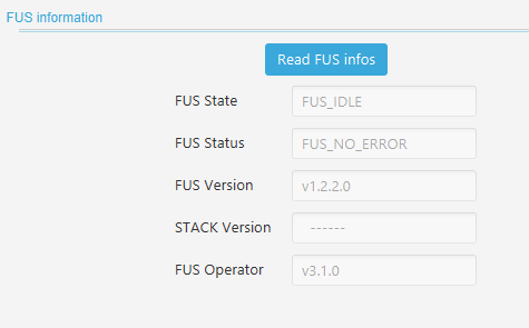
Reading the FUS information under section "Firmware Upgrade Service" gives the following result:

Trying to modify the option bytes with STM32CubeProgrammer yields the following result:
08:32:47 : Option byte command : -ob  BRSD_B=1  BRSD_A=1
  08:32:47 : PROGRAMMING OPTION BYTES AREA ...
  08:32:47 :   Bank          : 0x02
  08:32:47 :   Address       : 0x58004080
  08:32:47 :   Size          : 8 Bytes
  08:32:47 : Reconnecting...
  08:32:52 : Reconnected !
  08:32:52 : UPLOADING OPTION BYTES DATA ...
  08:32:52 :   Bank          : 0x00
  08:32:52 :   Address       : 0x58004020
  08:32:52 :   Size          : 60 Bytes
  08:32:52 :   Bank          : 0x01
  08:32:52 :   Address       : 0x5800403c
  08:32:52 :   Size          : 4 Bytes
  08:32:52 :   Bank          : 0x02
  08:32:52 :   Address       : 0x58004080
  08:32:52 :   Size          : 8 Bytes
  08:32:52 : OPTION BYTE PROGRAMMING VERIFICATION:
  08:32:52 : Error: Expected value for Option Byte "BRSD_A": 0x1, found: 0x0
  08:32:52 : Error: Expected value for Option Byte "BRSD_B": 0x1, found: 0x0
  08:32:52 : Error: Option Byte Programming failed
  08:32:52 : Time elapsed during option Bytes configuration: 00:00:05.487
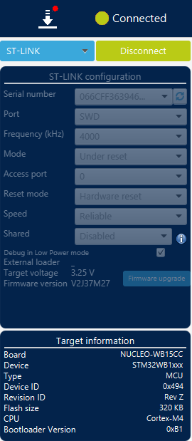
Just in case this could be a potential problem, here is information on my setup: 
- Mark as New
- Bookmark
- Subscribe
- Mute
- Subscribe to RSS Feed
- Permalink
- Email to a Friend
- Report Inappropriate Content
2023-06-06 12:43 AM
Update
After deleting the wireless stack once again on the Nucleo-WB15, the shown STACK-version remains "------", but now SRAM2a is unsecured. Although having access to SRAM2b would be nice, I think the combined size of SRAM1 (12KB) and SRAM2a (32KB) will be sufficient.
- Mark as New
- Bookmark
- Subscribe
- Mute
- Subscribe to RSS Feed
- Permalink
- Email to a Friend
- Report Inappropriate Content
2023-06-06 1:58 AM
Good!!
Anyhow, just to be more precise, FUS always keep one part of the SRAM2 for its own usage. This part will never be free for any application usage.
Note that BRSD_A and BRSD_B are part of the Secure SRAM2 start address and CPU2 reset vector option bytes which are only under CPU2 access control. You cannot write them => hence the error message you got.
SRAM2b is normally fully reserved for the wireless part but as you are not using it, you could be able to use it if you declare a new section in the linker fille that would be mapped from the SRAM2B_BASE address up to the SNBRSA address.
For more detail, please refer to AN5289 chapter 4.2 Memory mapping.
- STM32WBA63 + STM32_WPAN BLE + FreeRTOS tickless idle: BLE advertising misses LL timing after STOP wake when adding pre/post sleep hooks in STM32 MCUs Wireless
- STM32U3C5 - SMPS: Is an inductor needed for each VDD11? in STM32 MCUs Products
- STM32N657X0 NUCLEO — Secure LED not blinking, Non-Secure LED not working at all (TrustZone + RIF configuration issue) in STM32 MCUs Security
- STM32U575VGT: Autonomous SPI reading in STM32 MCUs Embedded software
- STM32H753 SPI6 Slave (H7 SPI v2) — Frame qualifies only with NSS-synchronised arming in STM32 MCUs Embedded software