- STMicroelectronics Community
- STM32 MCUs
- STM32 MCUs Products
- Solution: longer SPI cables via ''DualSPI''
- Subscribe to RSS Feed
- Mark Topic as New
- Mark Topic as Read
- Float this Topic for Current User
- Bookmark
- Subscribe
- Mute
- Printer Friendly Page
Solution: longer SPI cables via ''DualSPI''
- Mark as New
- Bookmark
- Subscribe
- Mute
- Subscribe to RSS Feed
- Permalink
- Email to a Friend
- Report Inappropriate Content
2018-06-21 4:12 PM
I'd like to share an idea, actually a working solution for a common issue:
''Why I cannot use a longer SPI cable?''''How can I make a SPI cable connection longer and keep still a high SPI speed/clock?''Issue:
Potentially, you know and have realized: when using SPI peripherals, the cable length to an external SPI device must be quite short. Often people think, it is caused by noise, reflection on the cable, missing shielding and not impedance matched. Sure, there are these issues but the main reason why SPI cable length is very limited:
SPI is a ''Synchronous'' (serial) Peripheral Interface.
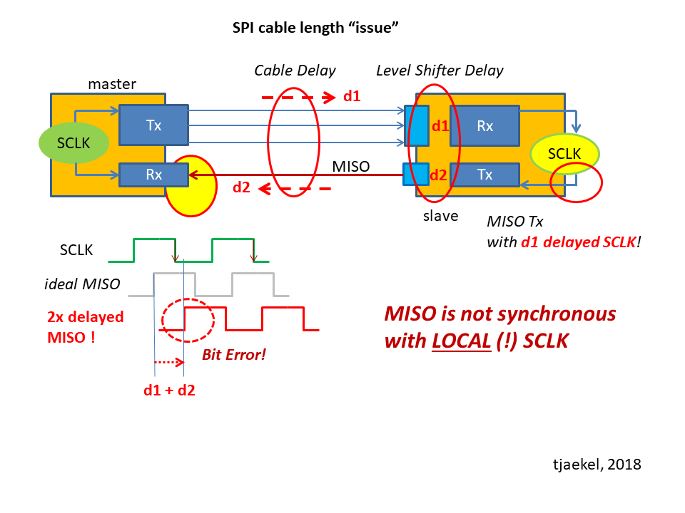
A master device will sample the incoming MISO from a slave with the same, internal (local !) SCLK. But the far end slave device sends MISO with the received, already delayed SCLK clock. And the MISO back to the master will be delayed again.So, the entire travel delay (in both directions) matters most. The cable delays (approx. 1 ns per 6 inches length) plus some buffers, line drivers or level shifters in the path (assume 4 ns per active buffers in path).
So, the MISO signal on the master receiver is ''not in sync'' anymore with the original (and internally used) SCLK for the Rx input shift register.
--> see figure 1
Solution:
''
Dual
SPI
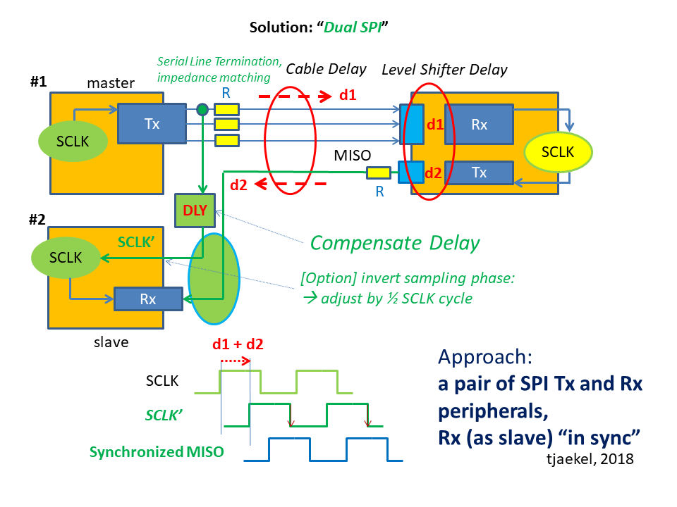
'': split your master SPI device into two separate and independent Tx and Rx peripherals. Use a pair of SPI Tx (master) and a SPI Rx as a slave in order to form your SPI device.So, your receiver can be fed with a delayed SCLK'. You can bring the MISO ''in sync'' again with the SCLK' signal. You have the option to compensate the delays (due to cable, due to buffers etc.).
So, we generate a delayed SCLK' signal and the slave Rx works now fine to sample MISO properly again.
How to create a delayed SCLK'?
You can use buffers, line drivers. Feed the SCLK from master through it. Use so many buffers that the sum of delays is approx. the entire delay of the SPI path (2x for both directions).Another ''trick'' (and option) you have:
The SPI Rx slave device is independent from the master. If you run a SPI mode X on master (Polarity and Phase config) - invert the SPI mode to Y for the slave (e.g. invert the clock phase on slave Rx).It gives you the option that the slave Rx will sample the incoming, delayed MISO with the ''opposite'' clock edge now. It gives you the option to delay (to ''shift'' signal) by one-half of SPI SCLK clock cycle.--> see figure 2

Comments:
I use this solution on a STM32H743 NUCLEO board: SPI 1 (as master, unidirectional Tx) is paired with SPI 4 (as a unidirectional Rx slave). The SCLK' delay is done by 2x Schmitt-Trigger buffers.
From a SW point of view - I use it still like a single bidirectional SPI device (send and receive via DMA done as one single function call).
I use also Schmitt-Triggers as line drivers, esp. also as the MISO receiver. And in addition: there is a Serial Line Termination:put resistors in series into the signal path. They should be placed as closest as possible to an output. And their value is the difference between the cable impedance + driver output impedance in order to match the impedance to the needed value. For instance: approx. 33R in order to match cable plus drivers for an entire impedance of 100..130 Ohm, for unbalanced ribbon cables.Results:
I could increase my SPI cable to approx.3 feet, with 26 MHz SPI clock
speed. Without this ''DualSPI'' I could achieve this speed just with few inches of cable. Or the long cable brings my working speed down to approx. 15 MHz.I have not tested how far I could go now. My guess: assuming you can delay via DLY block properly any amount of delay - now the cable length is just limited by noise, cross-talks and reflections. But the issue with the ''MISO not in sync'' should not be there anymore, never mind how long the cable is (just and unfortunately the amount of DLY depends on cable length). So, I assume I can make my cable now even longer with still the very high SPI clock speed kept.BTW: instead to do this local SCLK' feedback - you could also split the SCLK signal on the far end side and bring it back in the same way as the MISO signal from far end. This would make it independent of the cable length (a longer cable would adapt via itself for the needed SCLK' delay). You need just one addition SCLK' wire and it is not a really 4-signal standard SPI anymore. But if you have the option to bring SCLK back from far end SPI slave - it would be ''self-adapting''.
Suggestions for STM MCU HW designers:
The STM32H7xx has a great feature: the Delay Buffer DLYB. It can be used exactly for such purpose: delay a clock by N cycles, whereby N is configurable (as how many buffers, taps are used for the clock delay).
Unfortunately, this DLYB is hard-wired internally and can be used only for SDMMC or QSPI device.
--> it would be cool and great, if the pins (in + out) of DLYB would be available on external IO pins. So, I could feed my SCLK signal through the DLYB, configure the delay and bring my SCLK' signal to a receiver SPI input.
OK, it would still need external wires, connections, in order to route such a ''freely usable'' DLYB device.
Even fancier idea: if I could route the DLYB signals (in and out) or the IO pins where the signals would be available, to other IO signals - internally - this would be cool (no need for external connections).Example: if I could configure to take the SCLK SPI master output signal as an internal input the the DLYB, and the DLYB output as an SCLK input to another SPI (slave) device (also internally) - it would exactly do what I would need.So,
- if DLYB would be a freely usable block, with external IO's (like OPAMP)
- and if I could route even SPI signals to the DLYB, or to have a cross-connect matrix for IO pins (feed back an output as an input, but internally, for any combination of IOs)==> it would be really nice and cool. (actually I would need then 2x such DLYB because I want to use ''Dual SPI'' with two sets of SPI peripherals, 2x SPI connection needed, 3x SPI pairs potentially possible = 3x DLYB needed)
Please, have fun with the idea and working solution.
- Mark as New
- Bookmark
- Subscribe
- Mute
- Subscribe to RSS Feed
- Permalink
- Email to a Friend
- Report Inappropriate Content
2018-06-21 5:18 PM
SPI devices usually sample and shift on opposite edges so cable length delay is seldom a problem (galvanic isolation often is).
JW
- Mark as New
- Bookmark
- Subscribe
- Mute
- Subscribe to RSS Feed
- Permalink
- Email to a Friend
- Report Inappropriate Content
2018-06-26 7:02 PM
Sure, true: setup (change the value on MOSI) is with edge 1, sampling is with edge 2.
Bear in mind: if you have level shifters (4 ns per gate), or cable is quite long (1 ns per 6 inches) - you have remarkable delay.I did the test: with SCLK delay 'compensation' - you can get approx. the doubled speed.
The problem is that it starts with bit errors because the sampling on master Rx is not in sync anymore with the intended MISO.
BTW:
If you add galvanic isolation you might hit the same issue (and lower the max. SPI clock possible): you delay SCLK and MISO back to master (like level shifters). It improves just the signal-integrity in terms of signal levels (e.g. lower noise via GND, a better eye-diagram), not the issue due to delays (timing issue).- Unable to communicate with my Nucleo board using STM32CubeProgrammer in STM32CubeProgrammer (MCUs)
- STLINK-V3 MINIE V3J16M9 Firmware "STM32 Deubg+VCP" configuration non-functional VCP in STM32 MCUs Boards and hardware tools
- Nucleo-DRP1M1 with Nucleo-G0B1RE in STM32 MCUs Products
- Error in final launch sequence - No device on target in STM32CubeIDE (MCUs)
- stm32h503rbxx upload error in STM32 MCUs Products
