2026-05-09 9:28 PM - edited 2026-05-10 6:13 PM
I'm writing firmware for a development board based on the STM32H743 MCU, and I want to use an external GPIO input as the trigger or synchronization signal of DMAMUX to initiate DMA transactions. However, it seems that very little information is available on using GPIOs to start DMAs.
In the reference manual, "Table 127. DMAMUX2: assignment of trigger inputs to resources" and "Table 128. DMAMUX2: assignment of synchronization inputs to resources", it shows two trigger input signals: "Syscfg_exti0_mux" (number 20), and "Syscfg_exti2_mux" (number 21). So it seems to suggest that the EXTI trigger sources can indeed be used to trigger the DMA, but these two signals are not mentioned anywhere in the entire reference manual, there's no block diagram showing exactly what GPIO pins are connected. It says "SYSCFG" and "MUX", so they're probably the outputs controlled by programming SYSCFG_EXTICR1, SYSCFG_EXTICR2, SYSCFG_EXTICR3, SYSCFG_EXTICR4. But there are 4 EXTICRx and only two "exti_syscfg_extiX". It is unclear which is controlling which.
In "Table 103. DMAMUX2 and BDMA connections (continued)", again, two similar signals called "exti_syscfg_exti0" and "exti_syscfg_exti2" appear again, but mentioned nowhere in the reference manual elsewhere.
Likewise, in "Table 102. DMAMUX1, DMA1 and DMA2 connections (continued)", there's yet another signal called "exti_exti0_it", appearing once and mentioned nowhere. In "Table 103. DMAMUX2 and BDMA connections (continued)", there are two additional signals called "it_exti_exti0_syscfg", and "it_exti_exti2_syscfg", again, appearing once and mentioned nowhere.
The documentation quality on the EXTI interconnect is disappointing.
Question: What are the differences between "Syscfg_exti0_mux", "exti_syscfg_exti0", "exti_exti0_it", "it_exti_exti0_syscfg"? These output are generated by whom? How do I trigger the DMAMUX via a GPIO input?
Solved! Go to Solution.
2026-05-10 12:47 AM - edited 2026-05-16 7:52 AM
Indeed, my understanding is correct, syscfg_exti0_mux works exactly as what I expected.
1. The SYSCFG_EXTICRx registers provide 16 configuration 4-bit bitfields, each bitfield select a GPIO bank from A to K, the input pin must have the name number as the bitfield number. For example, bitfield 0 select the input GPIO bank of pin 0. This provides 16 multiplexed signal outputs EXTI[0:15].
2. Syscfg_extiX_mux is the raw output of EXTI[0:15]. Since only Syscfg_exti0_mux and Syscfg_exti2_mux are available as input, you can only use the signal EXTI[0] and EXTI[2], which correspond to GPIO[A:K] pin 0 and GPIO[A:K] pin 2. You cannot use other pins to trigger the DMA because of the lack of connections, but they don't need EXTI or NVIC.
Even better, because it's in the D3 domain, it keeps working autonomously even if the CPU core is halted in the debugger, or if the D1 domain is powered off completely. Unfortunately, only Pin 0 and Pin 2 of a GPIO bank can be used for that. For other pins you need to do it via a real peripheral.
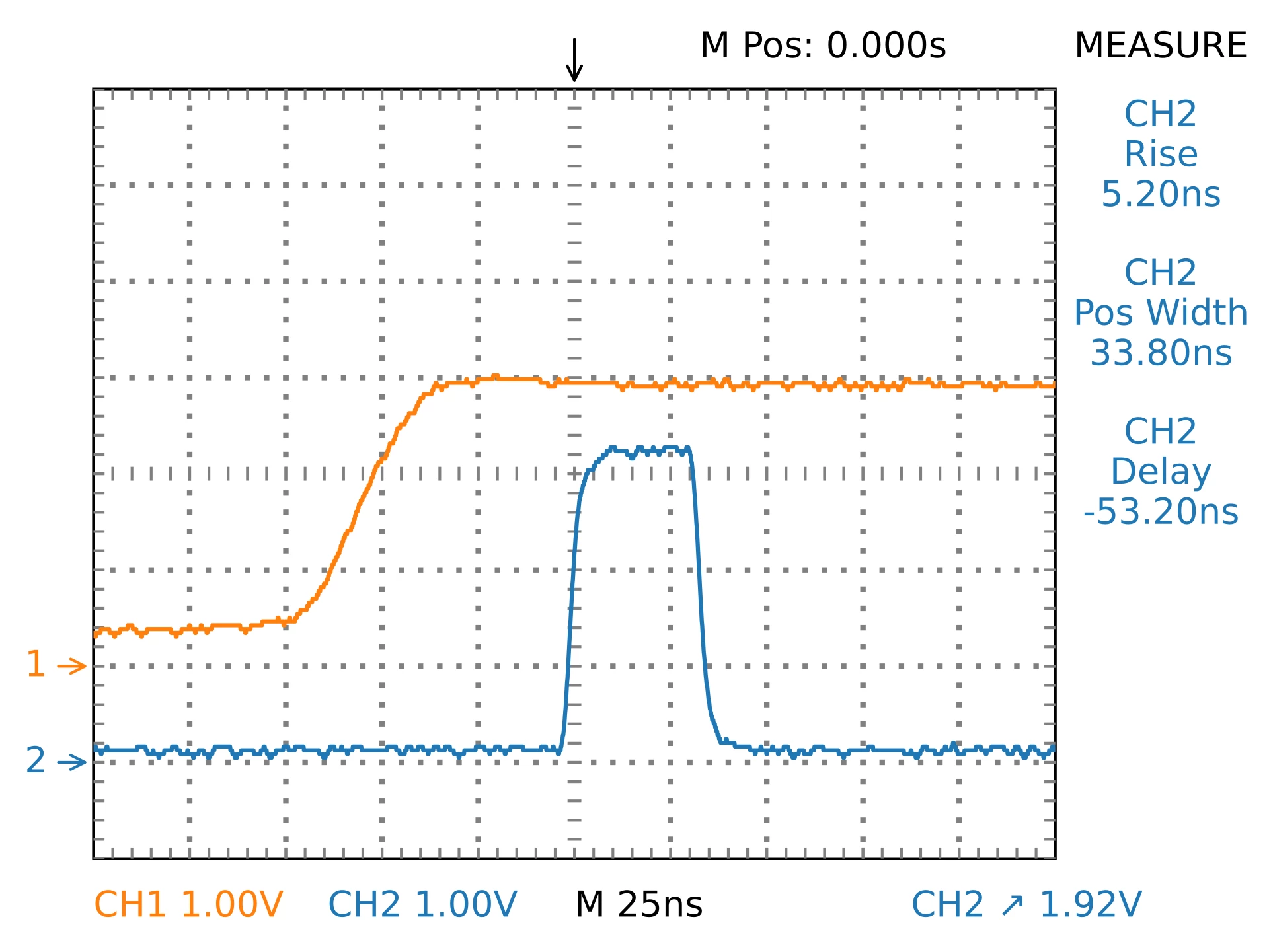
Using the following code:
static void bdma_config(void)
{
/*
* Select GPIO bank B as the source of the EXTI input line 0.
* GPIOB Pin 0 would generate a signal on EXTI Line 0.
*/
LL_SYSCFG_SetEXTISource(LL_SYSCFG_EXTI_PORTB, LL_SYSCFG_EXTI_LINE0);
LL_AHB4_GRP1_EnableClock(LL_AHB4_GRP1_PERIPH_BDMA);
/* Use EXTI line 0's rising edge to generate DMA Request 0 */
LL_DMAMUX_SetRequestSignalID(
DMAMUX2, LL_DMAMUX_REQ_GEN_0, LL_DMAMUX2_REQ_GEN_EXTI0
);
LL_DMAMUX_SetRequestGenPolarity(
DMAMUX2, LL_DMAMUX_REQ_GEN_0, LL_DMAMUX_REQ_GEN_POL_RISING
);
/* Trigger 2 DMA transfers per request */
LL_DMAMUX_SetGenRequestNb(DMAMUX2, LL_DMAMUX_REQ_GEN_0, 2);
LL_DMAMUX_EnableRequestGen(DMAMUX2, LL_DMAMUX_REQ_GEN_0);
__attribute__((section (".sram4_data")))
static const uint32_t gpio_data[] = { 0xFFFFFFFF, 0x00000000 };
static LL_BDMA_InitTypeDef bdma_ctx = {
.PeriphOrM2MSrcAddress = (uint32_t) &GPIOD->ODR,
.MemoryOrM2MDstAddress = (uint32_t) &gpio_data,
.Direction = LL_BDMA_DIRECTION_MEMORY_TO_PERIPH,
/* auto-reload if NbData goes to 0, otherwise DMA stops */
.Mode = LL_BDMA_MODE_CIRCULAR,
.PeriphOrM2MSrcIncMode = LL_BDMA_PERIPH_NOINCREMENT,
.MemoryOrM2MDstIncMode = LL_BDMA_MEMORY_INCREMENT,
.PeriphOrM2MSrcDataSize = LL_BDMA_PDATAALIGN_WORD,
.MemoryOrM2MDstDataSize = LL_BDMA_MDATAALIGN_WORD,
.NbData = sizeof(gpio_data) / sizeof(gpio_data[0]),
.PeriphRequest = LL_DMAMUX2_REQ_GENERATOR0,
.Priority = LL_BDMA_PRIORITY_VERYHIGH,
.DoubleBufferMode = LL_BDMA_DOUBLEBUFFER_MODE_DISABLE,
/* don't care */
.TargetMemInDoubleBufferMode = LL_BDMA_CURRENTTARGETMEM0,
};
LL_BDMA_Init(BDMA, LL_BDMA_CHANNEL_0, &bdma_ctx);
LL_BDMA_EnableChannel(BDMA, LL_BDMA_CHANNEL_0);
}
static void mainloop(void)
{
/*
* Set GPIO pin A9 as OUTPUT, this is connected to an LED on my devboard
* for indicating the firmware status. Can be removed.
*/
LL_GPIO_SetPinMode(GPIOA, LL_GPIO_PIN_9, LL_GPIO_MODE_OUTPUT);
LL_GPIO_SetOutputPin(GPIOA, LL_GPIO_PIN_9);
while (true) {
__NOP();
}
}
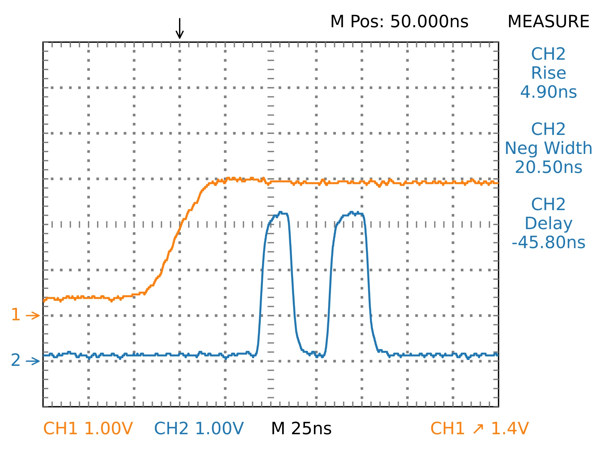
3. exti_exti0_it is the output of the EXTI interrupt controller, the same signal also goes to the CPU's NVIC. The same signal is connected to the DMAMUX controllers, which can use the interrupt's edge to initiate DMAs. But to use these signals to trigger DMA, EXTI's interrupt output to NVIC must also be enabled. This creates a problem: if you don't call LL_EXTI_ClearFlag, the EXTI's IRQ output line remains high, which means the DMA stops after the first rising edge.
So, after each DMA triggering, you either have to also enable an IRQ for the sole purpose of clearing this flag, or you have to clear the EXTI interrupt pending bit by polling, or by another DMA. This is why it's not recommended).
The following oscilloscope trace shows a working example:
Using the following code:
static void dma_config(void)
{
/*
* Select GPIO bank B as the source of the EXTI input line 0.
* GPIOB Pin 0 would generate a signal on EXTI Line 0.
*/
LL_SYSCFG_SetEXTISource(LL_SYSCFG_EXTI_PORTB, LL_SYSCFG_EXTI_LINE0);
/* Use EXTI Line 0 input's rising edge to trigger an IRQ. */
static LL_EXTI_InitTypeDef exti_ctx = {
.Line_0_31 = LL_EXTI_LINE_0,
.Line_32_63 = LL_EXTI_LINE_NONE,
.Line_64_95 = LL_EXTI_LINE_NONE,
.LineCommand = ENABLE,
.Mode = LL_EXTI_MODE_IT,
.Trigger = LL_EXTI_TRIGGER_RISING,
};
LL_EXTI_Init(&exti_ctx);
LL_AHB1_GRP1_EnableClock(LL_AHB1_GRP1_PERIPH_DMA1);
/* Use EXTI line 0's rising edge to generate DMA Request 0 */
LL_DMAMUX_SetRequestSignalID(
DMAMUX1, LL_DMAMUX_REQ_GEN_0, LL_DMAMUX1_REQ_GEN_EXTI0
);
LL_DMAMUX_SetRequestGenPolarity(
DMAMUX1, LL_DMAMUX_REQ_GEN_0, LL_DMAMUX_REQ_GEN_POL_RISING
);
/* Trigger 4 DMA transfers per request */
LL_DMAMUX_SetGenRequestNb(DMAMUX1, LL_DMAMUX_REQ_GEN_0, 4);
LL_DMAMUX_EnableRequestGen(DMAMUX1, LL_DMAMUX_REQ_GEN_0);
__attribute__((section (".sram1_data")))
static const uint32_t gpio_data[] = {
0xFFFFFFFF, 0x00000000, 0xFFFFFFFF, 0x00000000
};
static LL_DMA_InitTypeDef dma_ctx = {
.PeriphOrM2MSrcAddress = (uint32_t) &GPIOD->ODR,
.MemoryOrM2MDstAddress = (uint32_t) &gpio_data,
.Direction = LL_DMA_DIRECTION_MEMORY_TO_PERIPH,
.Mode = LL_DMA_MODE_CIRCULAR,
.PeriphOrM2MSrcIncMode = LL_DMA_PERIPH_NOINCREMENT,
.MemoryOrM2MDstIncMode = LL_DMA_MEMORY_INCREMENT,
.PeriphOrM2MSrcDataSize = LL_DMA_PDATAALIGN_WORD,
.MemoryOrM2MDstDataSize = LL_DMA_MDATAALIGN_WORD,
.NbData = sizeof(gpio_data) / sizeof(gpio_data[0]),
.PeriphRequest = LL_DMAMUX1_REQ_GENERATOR0,
.Priority = LL_DMA_PRIORITY_VERYHIGH,
.FIFOMode = LL_DMA_FIFOMODE_ENABLE,
.FIFOThreshold = LL_DMA_FIFOTHRESHOLD_FULL,
.MemBurst = LL_DMA_MBURST_INC4,
.PeriphBurst = LL_DMA_PBURST_SINGLE,
.DoubleBufferMode = LL_DMA_DOUBLEBUFFER_MODE_DISABLE,
/* don't care */
.TargetMemInDoubleBufferMode = LL_DMA_CURRENTTARGETMEM0,
};
LL_DMA_Init(DMA1, LL_DMA_STREAM_0, &dma_ctx);
LL_DMA_EnableStream(DMA1, LL_DMA_STREAM_0);
}
/*
* Use "noinline" to prevent this function from being inlined to main(),
* which is in Flash.
*/
__attribute__((section (".itcm_text"), noinline))
static void mainloop(void)
{
/*
* Set GPIO pin A9 as OUTPUT, this is connected to an LED on my devboard
* for indicating the firmware status. Can be removed.
*/
LL_GPIO_SetPinMode(GPIOA, LL_GPIO_PIN_9, LL_GPIO_MODE_OUTPUT);
LL_GPIO_SetOutputPin(GPIOA, LL_GPIO_PIN_9);
/*
* Because DMAMUX is edge-triggered by EXTI's IRQ output, not input, we
* must clear the EXTI flag LL_EXTI_ClearFlag_0_31(LL_EXTI_LINE_0); after
* every IRQ, otherwise the output flatlines and DMA stops. This can be
* done in a real ISR by enabling the IRQ.
*
* NVIC_SetPriority(EXTI0_IRQn, 0);
* NVIC_EnableIRQ(EXTI0_IRQn);
*
* Because we don't want the actual IRQ, NVIC is not enabled on this
* signal. But we still need to simulate the IRQ flag clearing
* by polling (or potentially another DMA transaction). This convoluted
* procedure is the reason that GPIO DMA triggering via EXTI is not
* recommended. Use another peripheral such as a timer if possible.
*/
while (true) {
/*
* Use WFI, not polling, because polling itself consumes bus
* bandwidth, which makes DMA transfer themselves if we're still
* polling during the DMA. If you must use polling, it's better
* to pull the NVIC, not the EXTI.
*
* NVIC_GetPendingIRQ(EXTI0_IRQn)
*
* // after LL_EXTI_ClearFlag_0_31 + 20 _NOP()
* NVIC_ClearPendingIRQ(EXTI0_IRQn)
*/
__WFI();
/* Clear IRQ flags immediately, otherwise DMA stops. */
LL_EXTI_ClearFlag_0_31(LL_EXTI_LINE_0);
/*
* The STM32H7 has a notorious "spurious IRQ" limitation because
* LL_*_ClearFlag() must travel across multiple buses and buffers
* with a long delay, causing the IRQ to retrigger. It can be worked
* around by clearing the IRQ flag early and relying on the natural
* ISR code delay. Adjust this delay if the CPU clock frequency or
* emulator performance changes. Always verify with an oscilloscope.
*
* http://efton.sk/STM32/gotcha/g7.html
*
*/
for (uint8_t i = 0; i < 20; i++) {
__NOP();
}
}
}Why should you use DMA1/DMA2 instead of BDMA? The D2 domain can access any memory, the D3 domain can only access SRAM4. Furthermore, the D2 domain's SRAM1 and DMA1 are faster than D3 domain's SRAM4 and BDMA (even though D2 still needs to access D3's GPIO controller). I'm not sure about the exact timing, but from the examples above, BDMA generates a GPIO pulse of 33 ns, but DMA1 generates a GPIO pulse of only 20 ns.
Furthermore, DMA1/DMA2 has a FIFO, which means the DMA doesn't need to access memory for every transfer, it can preload data and write that the destination in a burst. In this process, the DMA also uses the burst transfer type in the AHB protocol, reducing the latency between consecutive words.
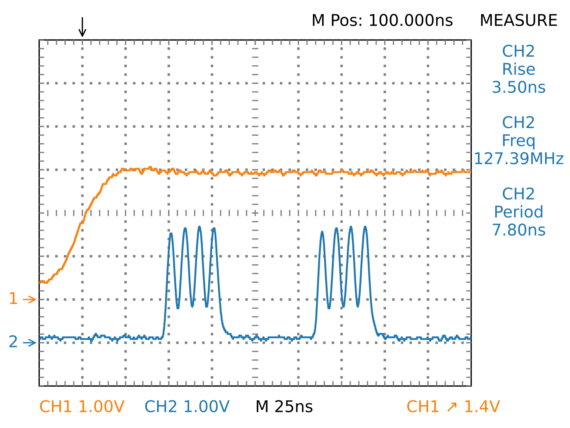
Here's an example of bitbanging GPIO via DMA1 using 8 16-bit burst, generating 8 transitions with a period of 7.8 ns, which is a frequency greater than 120 MHz! I think this is likely the fastest way to bitbang the GPIO on the STM32H7.
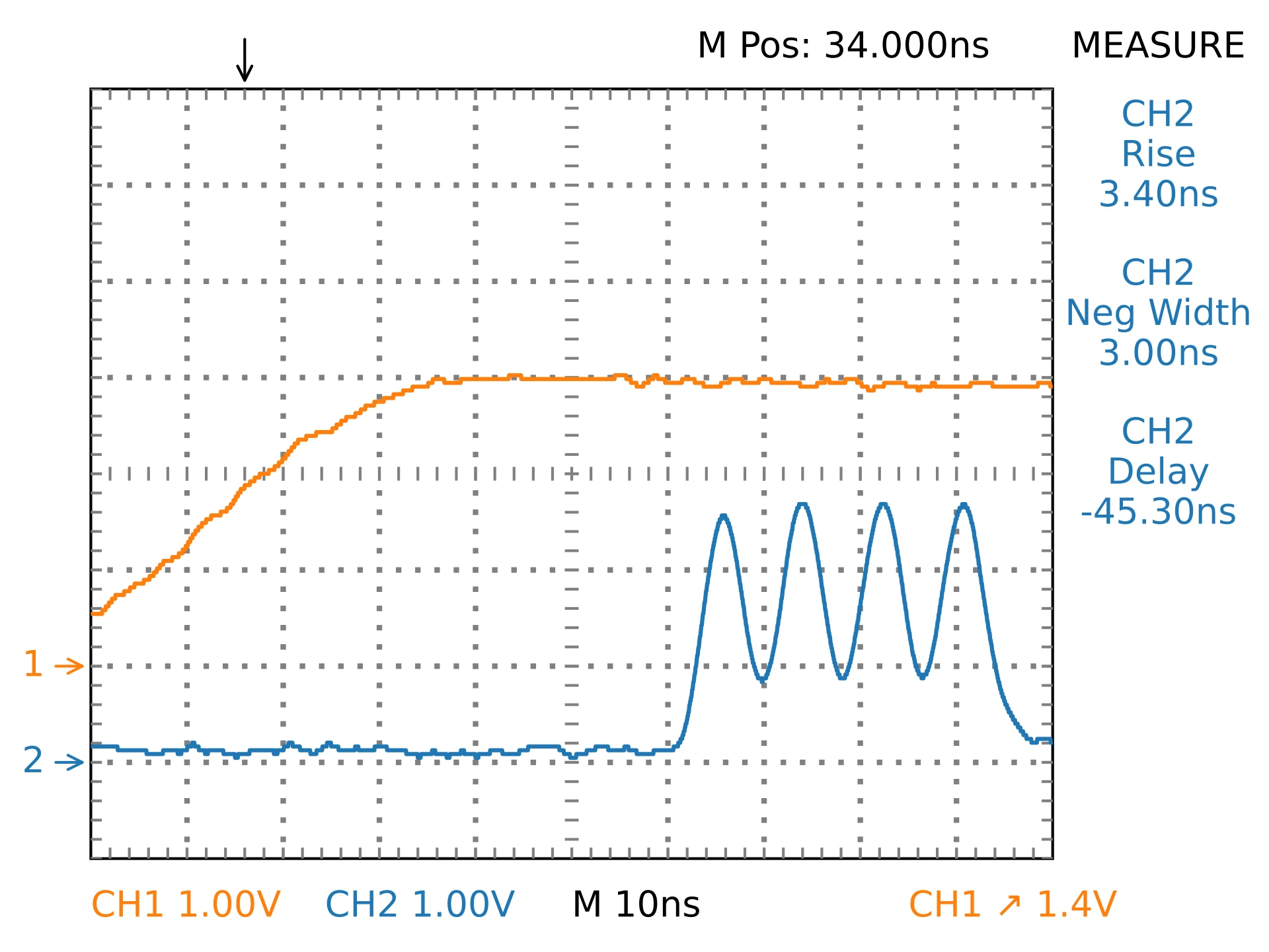
The number of pulses in the pulse train is limited to 4, 8, or 16. Note that time is needed to reload the DMA after each burst, the reloading time depends on the burst settings. In this example, it's 50 ns.
static void dma_config(void)
{
/*
* Select GPIO bank B as the source of the EXTI input line 0.
* GPIOB Pin 0 would generate a signal on EXTI Line 0.
*/
LL_SYSCFG_SetEXTISource(LL_SYSCFG_EXTI_PORTB, LL_SYSCFG_EXTI_LINE0);
/* Use EXTI Line 0 input's rising edge to trigger an IRQ. */
static LL_EXTI_InitTypeDef exti_ctx = {
.Line_0_31 = LL_EXTI_LINE_0,
.Line_32_63 = LL_EXTI_LINE_NONE,
.Line_64_95 = LL_EXTI_LINE_NONE,
.LineCommand = ENABLE,
.Mode = LL_EXTI_MODE_IT,
.Trigger = LL_EXTI_TRIGGER_RISING,
};
LL_EXTI_Init(&exti_ctx);
LL_AHB1_GRP1_EnableClock(LL_AHB1_GRP1_PERIPH_DMA1);
/* Use EXTI line 0's rising edge to generate DMA Request 0 */
LL_DMAMUX_SetRequestSignalID(
DMAMUX1, LL_DMAMUX_REQ_GEN_0, LL_DMAMUX1_REQ_GEN_EXTI0
);
LL_DMAMUX_SetRequestGenPolarity(
DMAMUX1, LL_DMAMUX_REQ_GEN_0, LL_DMAMUX_REQ_GEN_POL_RISING
);
LL_DMAMUX_SetGenRequestNb(DMAMUX1, LL_DMAMUX_REQ_GEN_0, 2);
LL_DMAMUX_EnableRequestGen(DMAMUX1, LL_DMAMUX_REQ_GEN_0);
__attribute__((section (".sram1_data")))
static const uint16_t gpio_data[] = {
0xFFFF, 0x0000, 0xFFFF, 0x0000,
};
static LL_DMA_InitTypeDef dma_ctx = {
.PeriphOrM2MSrcAddress = (uint32_t) &GPIOD->ODR,
.MemoryOrM2MDstAddress = (uint32_t) &gpio_data,
.Direction = LL_DMA_DIRECTION_MEMORY_TO_PERIPH,
.Mode = LL_DMA_MODE_CIRCULAR,
.PeriphOrM2MSrcIncMode = LL_DMA_PERIPH_NOINCREMENT,
.MemoryOrM2MDstIncMode = LL_DMA_MEMORY_INCREMENT,
.PeriphOrM2MSrcDataSize = LL_DMA_PDATAALIGN_HALFWORD,
.MemoryOrM2MDstDataSize = LL_DMA_MDATAALIGN_HALFWORD,
.NbData = sizeof(gpio_data) / sizeof(gpio_data[0]),
.PeriphRequest = LL_DMAMUX1_REQ_GENERATOR0,
.Priority = LL_DMA_PRIORITY_VERYHIGH,
.FIFOMode = LL_DMA_FIFOMODE_ENABLE,
.FIFOThreshold = LL_DMA_FIFOTHRESHOLD_FULL,
.MemBurst = LL_DMA_MBURST_INC8,
.PeriphBurst = LL_DMA_PBURST_INC8,
.DoubleBufferMode = LL_DMA_DOUBLEBUFFER_MODE_DISABLE,
/* don't care */
.TargetMemInDoubleBufferMode = LL_DMA_CURRENTTARGETMEM0,
};
LL_DMA_Init(DMA1, LL_DMA_STREAM_0, &dma_ctx);
LL_DMA_EnableStream(DMA1, LL_DMA_STREAM_0);
}Just make sure gpio_data is located in SRAM 1 (0x30000000) for DMA1, or SRAM 4 (0x38000000) for BDMA, may require custom startup and linker code. How to implement this is out of scope of this thread. I'm using a bare-metal environment, your mileage may vary.
What I do at startup:
void flash_to_mem(
char *flash_start,
volatile char *mem_start,
volatile char *mem_end
)
{
size_t len = mem_end - mem_start;
#ifdef SEMIHOSTING
printf(
"relocate %p-%p to %p, %d bytes\n",
flash_start,
flash_start + len,
mem_start,
len
);
#endif
/*
* Language Lawyering.
*
* Don't use memcpy(). This is widely used in embedded libraries, but it's
* a theoretical Undefined Behavior as C compilers can remove memcpy()
* when they don't have any visible effects to C code under the "as-if"
* rule. Mark destination variables as "volatile char *", and copy manual-
* ly. Keyword "volatile" ensures it's always executed, and "char *" is
* the only data type in C that is safe to cast into without breaking
* aliasing or alignment rules (even "uint8_t *" does not enjoy this
* exception).
*/
for (size_t i = 0; i < len; i++) {
mem_start[i] = flash_start[i];
}
}
void relocate_to_itcm(void)
{
extern char _si_isr_vector;
extern volatile char __isr_vector_start, __isr_vector_end;
flash_to_mem(&_si_isr_vector, &__isr_vector_start, &__isr_vector_end);
extern char _si_itcm_text;
extern volatile char __itcm_text_start, __itcm_text_end;
flash_to_mem(&_si_itcm_text, &__itcm_text_start, &__itcm_text_end);
SCB->VTOR = D1_ITCMRAM_BASE;
/*
* Test memory access latency by declaring arrays with:
*
* __attribute__((section (".axisram_data")))
* __attribute__((section (".sram1_data")))
* __attribute__((section (".sram2_data")))
* __attribute__((section (".sram3_data")))
* __attribute__((section (".sram4_data")))
*
* Note that different SRAMs have different access latency due
* to their bus locations. Some peripherals can only read from
* a specific SRAM bank (e.g. BDMA can only read from SRAM4).
*
* Not used in this example, can be removed.
*/
extern char _si_axisram_data;
extern volatile char __axisram_data_start, __axisram_data_end;
LL_AHB3_GRP1_EnableClock(LL_AHB3_GRP1_PERIPH_AXISRAM);
flash_to_mem(
&_si_axisram_data, &__axisram_data_start, &__axisram_data_end
);
extern char _si_sram1_data;
extern volatile char __sram1_data_start, __sram1_data_end;
LL_AHB2_GRP1_EnableClock(LL_AHB2_GRP1_PERIPH_D2SRAM1);
flash_to_mem(&_si_sram1_data, &__sram1_data_start, &__sram1_data_end);
extern char _si_sram2_data;
extern volatile char __sram2_data_start, __sram2_data_end;
LL_AHB2_GRP1_EnableClock(LL_AHB2_GRP1_PERIPH_D2SRAM2);
flash_to_mem(&_si_sram2_data, &__sram2_data_start, &__sram2_data_end);
extern char _si_sram3_data;
extern volatile char __sram3_data_start, __sram3_data_end;
LL_AHB2_GRP1_EnableClock(LL_AHB2_GRP1_PERIPH_D2SRAM3);
flash_to_mem(&_si_sram3_data, &__sram3_data_start, &__sram3_data_end);
extern char _si_sram4_data;
extern volatile char __sram4_data_start, __sram4_data_end;
LL_AHB4_GRP1_EnableClock(LL_AHB4_GRP1_PERIPH_SRAM4);
flash_to_mem(&_si_sram4_data, &__sram4_data_start, &__sram4_data_end);
}Using the following linker file:
/* SPDX-License-Identifier: Apache-2.0 AND (0BSD OR CC0-1.0) */
/*
******************************************************************************
**
** File : LinkerScript.ld
**
**
** Abstract : Linker script for STM32H7 series
** 2048Kbytes FLASH, 64Kbytes ITCMRAM, 128Kbytes DTCMRAM
**
** Set heap size, stack size and stack location according
** to application requirements.
**
** Set memory bank area and size if external memory is used.
**
** Target : STMicroelectronics STM32
**
** Distribution: The file is distributed as is without any warranty
** of any kind.
**
*****************************************************************************
** @attention
**
** Copyright (C) 2026 niconiconi.
**
** Modified from stm32h745xx_flash_CM7.ld to stm32h743xx_flash_CM7.ld,
** for STM32H7 support, including project-specific ITCM/DTCM customizations.
**
** This file is free software: you may copy, redistribute and/or modify it
** under the terms of the BSD Zero Clause License, or (at your option)
** Creative Commons Zero v1.0 Universal license. See "SPDX-License-Identifier"
** for more details.
**
** This file is distributed in the hope that it will be useful, but WITHOUT ANY
** WARRANTY; without even the implied warranty of MERCHANTABILITY or FITNESS
** FOR A PARTICULAR PURPOSE.
**
** This file incorporates work covered by the following copyright and
** permission notice:
**
** Copyright (c) 2019 STMicroelectronics.
** All rights reserved.
**
** This software is licensed under terms that can be found in the LICENSE
** file in the root directory of this software component. If no LICENSE
** file comes with this software, it is provided AS-IS.
**
** LICENSE file in the root directory of the origin:
**
** Component: CMSIS Device
** Copyright: ARM Limited, STMicroelectronics
** License: Apache License 2.0
**
******************************************************************************
*/
/* Entry Point */
ENTRY(Reset_Handler)
/* Highest address of the user mode stack */
_estack = 0x20020000; /* end of RAM */
/* Generate a link error if heap and stack don't fit into RAM */
_Min_Heap_Size = 0x200; /* required amount of heap */
_Min_Stack_Size = 0x400; /* required amount of stack */
/* Specify the memory areas */
MEMORY
{
FLASH (rx) : ORIGIN = 0x08000000, LENGTH = 2048K
ITCMRAM (xrw) : ORIGIN = 0x00000000, LENGTH = 64K
DTCMRAM (xrw) : ORIGIN = 0x20000000, LENGTH = 128K
AXISRAM (rw) : ORIGIN = 0x24000000, LENGTH = 512K
SRAM1 (rw) : ORIGIN = 0x30000000, LENGTH = 128K
SRAM2 (rw) : ORIGIN = 0x30020000, LENGTH = 128K
SRAM3 (rw) : ORIGIN = 0x30040000, LENGTH = 32K
SRAM4 (rw) : ORIGIN = 0x38000000, LENGTH = 64K
}
/* Define output sections */
SECTIONS
{
/* The startup code goes into ITCM (relocated from FLASH) */
.isr_vector :
{
. = ALIGN(4);
__isr_vector_start = .;
KEEP(*(.isr_vector)) /* Startup code */
. = ALIGN(4);
__isr_vector_end = .;
} >ITCMRAM AT> FLASH
.itcm_text :
{
. = ALIGN(4);
__itcm_text_start = .;
*(.itcm_text)
*(.itcm_text*)
. = ALIGN(4);
__itcm_text_end = .;
} > ITCMRAM AT> FLASH
/* used by the startup to initialize data */
_si_isr_vector = LOADADDR(.isr_vector);
_si_itcm_text = LOADADDR(".itcm_text");
/* The program code and other data goes into FLASH */
.text :
{
. = ALIGN(4);
*(.text) /* .text sections (code) */
*(.text*) /* .text* sections (code) */
*(.glue_7) /* glue arm to thumb code */
*(.glue_7t) /* glue thumb to arm code */
*(.eh_frame)
KEEP (*(.init))
KEEP (*(.fini))
. = ALIGN(4);
_etext = .; /* define a global symbols at end of code */
} >FLASH
/* Constant data goes into FLASH */
.rodata :
{
. = ALIGN(4);
*(.rodata) /* .rodata sections (constants, strings, etc.) */
*(.rodata*) /* .rodata* sections (constants, strings, etc.) */
. = ALIGN(4);
} >FLASH
.ARM.extab (READONLY) : /* The READONLY keyword is only supported in GCC11 and later, remove it if using GCC10 or earlier. */
{
. = ALIGN(4);
*(.ARM.extab* .gnu.linkonce.armextab.*)
. = ALIGN(4);
} >FLASH
.ARM (READONLY) : /* The READONLY keyword is only supported in GCC11 and later, remove it if using GCC10 or earlier. */
{
. = ALIGN(4);
__exidx_start = .;
*(.ARM.exidx*)
__exidx_end = .;
. = ALIGN(4);
} >FLASH
.preinit_array (READONLY) : /* The READONLY keyword is only supported in GCC11 and later, remove it if using GCC10 or earlier. */
{
. = ALIGN(4);
PROVIDE_HIDDEN (__preinit_array_start = .);
KEEP (*(.preinit_array*))
PROVIDE_HIDDEN (__preinit_array_end = .);
. = ALIGN(4);
} >FLASH
.init_array (READONLY) : /* The READONLY keyword is only supported in GCC11 and later, remove it if using GCC10 or earlier. */
{
. = ALIGN(4);
PROVIDE_HIDDEN (__init_array_start = .);
KEEP (*(SORT(.init_array.*)))
KEEP (*(.init_array*))
PROVIDE_HIDDEN (__init_array_end = .);
. = ALIGN(4);
} >FLASH
.fini_array (READONLY) : /* The READONLY keyword is only supported in GCC11 and later, remove it if using GCC10 or earlier. */
{
. = ALIGN(4);
PROVIDE_HIDDEN (__fini_array_start = .);
KEEP (*(SORT(.fini_array.*)))
KEEP (*(.fini_array*))
PROVIDE_HIDDEN (__fini_array_end = .);
. = ALIGN(4);
} >FLASH
/* used by the startup to initialize data */
_sidata = LOADADDR(.data);
_si_sram1_data = LOADADDR(.sram1_data);
_si_sram2_data = LOADADDR(.sram2_data);
_si_sram3_data = LOADADDR(.sram3_data);
_si_sram4_data = LOADADDR(.sram4_data);
_si_axisram_data = LOADADDR(.axisram_data);
/* Initialized data sections goes into RAM, load LMA copy after code */
.data :
{
. = ALIGN(4);
_sdata = .; /* create a global symbol at data start */
*(.data) /* .data sections */
*(.data*) /* .data* sections */
. = ALIGN(4);
_edata = .; /* define a global symbol at data end */
} >DTCMRAM AT> FLASH
.axisram_data :
{
. = ALIGN(4);
__axisram_data_start = .;
*(.axisram_data)
*(.axisram_data*)
. = ALIGN(4);
__axisram_data_end = .;
} >AXISRAM AT> FLASH
.sram1_data :
{
. = ALIGN(4);
__sram1_data_start = .;
*(.sram1_data)
*(.sram1_data*)
. = ALIGN(4);
__sram1_data_end = .;
} >SRAM1 AT> FLASH
.sram2_data :
{
. = ALIGN(4);
__sram2_data_start = .;
*(.sram2_data)
*(.sram2_data*)
. = ALIGN(4);
__sram2_data_end = .;
} >SRAM2 AT> FLASH
.sram3_data :
{
. = ALIGN(4);
__sram3_data_start = .;
*(.sram3_data)
*(.sram3_data*)
. = ALIGN(4);
__sram3_data_end = .;
} >SRAM3 AT> FLASH
.sram4_data :
{
. = ALIGN(4);
__sram4_data_start = .;
*(.sram4_data)
*(.sram4_data*)
. = ALIGN(4);
__sram4_data_end = .;
} >SRAM4 AT> FLASH
/* Uninitialized data section */
. = ALIGN(4);
.bss :
{
/* This is used by the startup in order to initialize the .bss section */
_sbss = .; /* define a global symbol at bss start */
__bss_start__ = _sbss;
*(.bss)
*(.bss*)
*(COMMON)
. = ALIGN(4);
_ebss = .; /* define a global symbol at bss end */
__bss_end__ = _ebss;
} >DTCMRAM
/* User_heap_stack section, used to check that there is enough RAM left */
._user_heap_stack :
{
. = ALIGN(8);
PROVIDE ( end = . );
PROVIDE ( _end = . );
. = . + _Min_Heap_Size;
. = . + _Min_Stack_Size;
. = ALIGN(8);
} >DTCMRAM
/* Remove information from the standard libraries */
/DISCARD/ :
{
libc.a ( * )
libm.a ( * )
libgcc.a ( * )
}
.ARM.attributes 0 : { *(.ARM.attributes) }
}
2026-05-09 10:41 PM - edited 2026-05-09 11:11 PM
The only mention of the signal "Syscfg_exti0_mux" on the entire Web was on a Chinese forum (called "Rough Guy Embedded"), which seems to provide a clue. The OP said,
Using EXTI0 to trigger BDMA to transfer data input from the GPIO port to SRAM4 works normally. However, if EXTI0 is used to trigger DMA1 and DMA2 to transfer data input from the GPIO port to SRAM1~2, the DMA fails to start. A clue was found: In Table 117 of section 16.3.2 DMAMUX1 mapping in the H7 reference manual RM0433 V5, DMAMUX1 Trigger input #6 is marked as “extit0”. Meanwhile, Table 119 of section 16.3.3 DMAMUX2 mapping shows DMAMUX2 Trigger input #20 as “Syscfg_exti0_mux”.
Could this be the reason why BDMA using DMAMUX2 can be triggered by EXTI0, while DMA1~2 using DMAMUX1 cannot? I'd like to ask the gurus: does anyone know the details of the "extit0" and "Syscfg_exti0_mux" signals? I've searched the entire manual but can't find any source or description.
The reply suggested:
The interrupt should be enabled, it only works if you can enter the EXTI0_IRQHandler.
HAL_NVIC_SetPriority(EXTI0_IRQn, 0, 0);
HAL_NVIC_EnableIRQ(EXTI0_IRQn);
From another thread on this forum, Make EXTI generates a request to DMA1 on STM32H7, the OP was also able to get a statement from ST that:
The behaviour with the EXTI0 is different in domain D3 (triggering BDMA from EXTI0). This is due to the fact that the domain D3 is designed for autonomous mode where both CPU core are OFF. The EXTI0 can only be used as an event. It is automatically cleared.
With DMAMUX1 in domain D2, if a trigger is needed without executing an IRQ handler, the EXTI0 is not the good one. A timer or a DMA event has to be used instead.
So putting everything together...
If my understanding is correct, I think this is what happens:
1. The SYSCFG_EXTICRx registers provide 16 configuration 4-bit bitfields, each bitfield select a GPIO bank from A to K, the input pin must have the name number as the bitfield number. For example, bitfield 0 select the input GPIO bank of pin 0. This provides 16 multiplexed signal outputs EXTI[0:15].
2. Syscfg_extiX_mux is the raw output of EXTI[0:15]. Since only Syscfg_exti0_mux and Syscfg_exti2_mux are available as input, you can only use the signal EXTI[0] and EXTI[2], which correspond to GPIO[A:K] pin 0 and GPIO[A:K] pin 2. You cannot use other pins to trigger the DMA because of the lack of connections, but they don't need EXTI or NVIC.
3. exti_exti0_it is the output of the EXTI interrupt controller, the same signal also goes to the CPU's NVIC. The same signal is connected to some DMA controllers can use the interrupt to initiate DMA. But to use these signals to trigger DMA, EXTI's interrupt output to NVIC must also be enabled. So you either have to accept an IRQ as a side-effect, or enable IRQ on the EXTI but mask that IRQ on the NVIC (but then you have to find a way to clear the EXTI interrupt pending bit, otherwise this line remains active - which is why it's not recommended).
Hopefully I got everything right.
2026-05-10 12:47 AM - edited 2026-05-16 7:52 AM
Indeed, my understanding is correct, syscfg_exti0_mux works exactly as what I expected.
1. The SYSCFG_EXTICRx registers provide 16 configuration 4-bit bitfields, each bitfield select a GPIO bank from A to K, the input pin must have the name number as the bitfield number. For example, bitfield 0 select the input GPIO bank of pin 0. This provides 16 multiplexed signal outputs EXTI[0:15].
2. Syscfg_extiX_mux is the raw output of EXTI[0:15]. Since only Syscfg_exti0_mux and Syscfg_exti2_mux are available as input, you can only use the signal EXTI[0] and EXTI[2], which correspond to GPIO[A:K] pin 0 and GPIO[A:K] pin 2. You cannot use other pins to trigger the DMA because of the lack of connections, but they don't need EXTI or NVIC.
Even better, because it's in the D3 domain, it keeps working autonomously even if the CPU core is halted in the debugger, or if the D1 domain is powered off completely. Unfortunately, only Pin 0 and Pin 2 of a GPIO bank can be used for that. For other pins you need to do it via a real peripheral.
Using the following code:
static void bdma_config(void)
{
/*
* Select GPIO bank B as the source of the EXTI input line 0.
* GPIOB Pin 0 would generate a signal on EXTI Line 0.
*/
LL_SYSCFG_SetEXTISource(LL_SYSCFG_EXTI_PORTB, LL_SYSCFG_EXTI_LINE0);
LL_AHB4_GRP1_EnableClock(LL_AHB4_GRP1_PERIPH_BDMA);
/* Use EXTI line 0's rising edge to generate DMA Request 0 */
LL_DMAMUX_SetRequestSignalID(
DMAMUX2, LL_DMAMUX_REQ_GEN_0, LL_DMAMUX2_REQ_GEN_EXTI0
);
LL_DMAMUX_SetRequestGenPolarity(
DMAMUX2, LL_DMAMUX_REQ_GEN_0, LL_DMAMUX_REQ_GEN_POL_RISING
);
/* Trigger 2 DMA transfers per request */
LL_DMAMUX_SetGenRequestNb(DMAMUX2, LL_DMAMUX_REQ_GEN_0, 2);
LL_DMAMUX_EnableRequestGen(DMAMUX2, LL_DMAMUX_REQ_GEN_0);
__attribute__((section (".sram4_data")))
static const uint32_t gpio_data[] = { 0xFFFFFFFF, 0x00000000 };
static LL_BDMA_InitTypeDef bdma_ctx = {
.PeriphOrM2MSrcAddress = (uint32_t) &GPIOD->ODR,
.MemoryOrM2MDstAddress = (uint32_t) &gpio_data,
.Direction = LL_BDMA_DIRECTION_MEMORY_TO_PERIPH,
/* auto-reload if NbData goes to 0, otherwise DMA stops */
.Mode = LL_BDMA_MODE_CIRCULAR,
.PeriphOrM2MSrcIncMode = LL_BDMA_PERIPH_NOINCREMENT,
.MemoryOrM2MDstIncMode = LL_BDMA_MEMORY_INCREMENT,
.PeriphOrM2MSrcDataSize = LL_BDMA_PDATAALIGN_WORD,
.MemoryOrM2MDstDataSize = LL_BDMA_MDATAALIGN_WORD,
.NbData = sizeof(gpio_data) / sizeof(gpio_data[0]),
.PeriphRequest = LL_DMAMUX2_REQ_GENERATOR0,
.Priority = LL_BDMA_PRIORITY_VERYHIGH,
.DoubleBufferMode = LL_BDMA_DOUBLEBUFFER_MODE_DISABLE,
/* don't care */
.TargetMemInDoubleBufferMode = LL_BDMA_CURRENTTARGETMEM0,
};
LL_BDMA_Init(BDMA, LL_BDMA_CHANNEL_0, &bdma_ctx);
LL_BDMA_EnableChannel(BDMA, LL_BDMA_CHANNEL_0);
}
static void mainloop(void)
{
/*
* Set GPIO pin A9 as OUTPUT, this is connected to an LED on my devboard
* for indicating the firmware status. Can be removed.
*/
LL_GPIO_SetPinMode(GPIOA, LL_GPIO_PIN_9, LL_GPIO_MODE_OUTPUT);
LL_GPIO_SetOutputPin(GPIOA, LL_GPIO_PIN_9);
while (true) {
__NOP();
}
}
3. exti_exti0_it is the output of the EXTI interrupt controller, the same signal also goes to the CPU's NVIC. The same signal is connected to the DMAMUX controllers, which can use the interrupt's edge to initiate DMAs. But to use these signals to trigger DMA, EXTI's interrupt output to NVIC must also be enabled. This creates a problem: if you don't call LL_EXTI_ClearFlag, the EXTI's IRQ output line remains high, which means the DMA stops after the first rising edge.
So, after each DMA triggering, you either have to also enable an IRQ for the sole purpose of clearing this flag, or you have to clear the EXTI interrupt pending bit by polling, or by another DMA. This is why it's not recommended).
The following oscilloscope trace shows a working example:
Using the following code:
static void dma_config(void)
{
/*
* Select GPIO bank B as the source of the EXTI input line 0.
* GPIOB Pin 0 would generate a signal on EXTI Line 0.
*/
LL_SYSCFG_SetEXTISource(LL_SYSCFG_EXTI_PORTB, LL_SYSCFG_EXTI_LINE0);
/* Use EXTI Line 0 input's rising edge to trigger an IRQ. */
static LL_EXTI_InitTypeDef exti_ctx = {
.Line_0_31 = LL_EXTI_LINE_0,
.Line_32_63 = LL_EXTI_LINE_NONE,
.Line_64_95 = LL_EXTI_LINE_NONE,
.LineCommand = ENABLE,
.Mode = LL_EXTI_MODE_IT,
.Trigger = LL_EXTI_TRIGGER_RISING,
};
LL_EXTI_Init(&exti_ctx);
LL_AHB1_GRP1_EnableClock(LL_AHB1_GRP1_PERIPH_DMA1);
/* Use EXTI line 0's rising edge to generate DMA Request 0 */
LL_DMAMUX_SetRequestSignalID(
DMAMUX1, LL_DMAMUX_REQ_GEN_0, LL_DMAMUX1_REQ_GEN_EXTI0
);
LL_DMAMUX_SetRequestGenPolarity(
DMAMUX1, LL_DMAMUX_REQ_GEN_0, LL_DMAMUX_REQ_GEN_POL_RISING
);
/* Trigger 4 DMA transfers per request */
LL_DMAMUX_SetGenRequestNb(DMAMUX1, LL_DMAMUX_REQ_GEN_0, 4);
LL_DMAMUX_EnableRequestGen(DMAMUX1, LL_DMAMUX_REQ_GEN_0);
__attribute__((section (".sram1_data")))
static const uint32_t gpio_data[] = {
0xFFFFFFFF, 0x00000000, 0xFFFFFFFF, 0x00000000
};
static LL_DMA_InitTypeDef dma_ctx = {
.PeriphOrM2MSrcAddress = (uint32_t) &GPIOD->ODR,
.MemoryOrM2MDstAddress = (uint32_t) &gpio_data,
.Direction = LL_DMA_DIRECTION_MEMORY_TO_PERIPH,
.Mode = LL_DMA_MODE_CIRCULAR,
.PeriphOrM2MSrcIncMode = LL_DMA_PERIPH_NOINCREMENT,
.MemoryOrM2MDstIncMode = LL_DMA_MEMORY_INCREMENT,
.PeriphOrM2MSrcDataSize = LL_DMA_PDATAALIGN_WORD,
.MemoryOrM2MDstDataSize = LL_DMA_MDATAALIGN_WORD,
.NbData = sizeof(gpio_data) / sizeof(gpio_data[0]),
.PeriphRequest = LL_DMAMUX1_REQ_GENERATOR0,
.Priority = LL_DMA_PRIORITY_VERYHIGH,
.FIFOMode = LL_DMA_FIFOMODE_ENABLE,
.FIFOThreshold = LL_DMA_FIFOTHRESHOLD_FULL,
.MemBurst = LL_DMA_MBURST_INC4,
.PeriphBurst = LL_DMA_PBURST_SINGLE,
.DoubleBufferMode = LL_DMA_DOUBLEBUFFER_MODE_DISABLE,
/* don't care */
.TargetMemInDoubleBufferMode = LL_DMA_CURRENTTARGETMEM0,
};
LL_DMA_Init(DMA1, LL_DMA_STREAM_0, &dma_ctx);
LL_DMA_EnableStream(DMA1, LL_DMA_STREAM_0);
}
/*
* Use "noinline" to prevent this function from being inlined to main(),
* which is in Flash.
*/
__attribute__((section (".itcm_text"), noinline))
static void mainloop(void)
{
/*
* Set GPIO pin A9 as OUTPUT, this is connected to an LED on my devboard
* for indicating the firmware status. Can be removed.
*/
LL_GPIO_SetPinMode(GPIOA, LL_GPIO_PIN_9, LL_GPIO_MODE_OUTPUT);
LL_GPIO_SetOutputPin(GPIOA, LL_GPIO_PIN_9);
/*
* Because DMAMUX is edge-triggered by EXTI's IRQ output, not input, we
* must clear the EXTI flag LL_EXTI_ClearFlag_0_31(LL_EXTI_LINE_0); after
* every IRQ, otherwise the output flatlines and DMA stops. This can be
* done in a real ISR by enabling the IRQ.
*
* NVIC_SetPriority(EXTI0_IRQn, 0);
* NVIC_EnableIRQ(EXTI0_IRQn);
*
* Because we don't want the actual IRQ, NVIC is not enabled on this
* signal. But we still need to simulate the IRQ flag clearing
* by polling (or potentially another DMA transaction). This convoluted
* procedure is the reason that GPIO DMA triggering via EXTI is not
* recommended. Use another peripheral such as a timer if possible.
*/
while (true) {
/*
* Use WFI, not polling, because polling itself consumes bus
* bandwidth, which makes DMA transfer themselves if we're still
* polling during the DMA. If you must use polling, it's better
* to pull the NVIC, not the EXTI.
*
* NVIC_GetPendingIRQ(EXTI0_IRQn)
*
* // after LL_EXTI_ClearFlag_0_31 + 20 _NOP()
* NVIC_ClearPendingIRQ(EXTI0_IRQn)
*/
__WFI();
/* Clear IRQ flags immediately, otherwise DMA stops. */
LL_EXTI_ClearFlag_0_31(LL_EXTI_LINE_0);
/*
* The STM32H7 has a notorious "spurious IRQ" limitation because
* LL_*_ClearFlag() must travel across multiple buses and buffers
* with a long delay, causing the IRQ to retrigger. It can be worked
* around by clearing the IRQ flag early and relying on the natural
* ISR code delay. Adjust this delay if the CPU clock frequency or
* emulator performance changes. Always verify with an oscilloscope.
*
* http://efton.sk/STM32/gotcha/g7.html
*
*/
for (uint8_t i = 0; i < 20; i++) {
__NOP();
}
}
}Why should you use DMA1/DMA2 instead of BDMA? The D2 domain can access any memory, the D3 domain can only access SRAM4. Furthermore, the D2 domain's SRAM1 and DMA1 are faster than D3 domain's SRAM4 and BDMA (even though D2 still needs to access D3's GPIO controller). I'm not sure about the exact timing, but from the examples above, BDMA generates a GPIO pulse of 33 ns, but DMA1 generates a GPIO pulse of only 20 ns.
Furthermore, DMA1/DMA2 has a FIFO, which means the DMA doesn't need to access memory for every transfer, it can preload data and write that the destination in a burst. In this process, the DMA also uses the burst transfer type in the AHB protocol, reducing the latency between consecutive words.
Here's an example of bitbanging GPIO via DMA1 using 8 16-bit burst, generating 8 transitions with a period of 7.8 ns, which is a frequency greater than 120 MHz! I think this is likely the fastest way to bitbang the GPIO on the STM32H7.
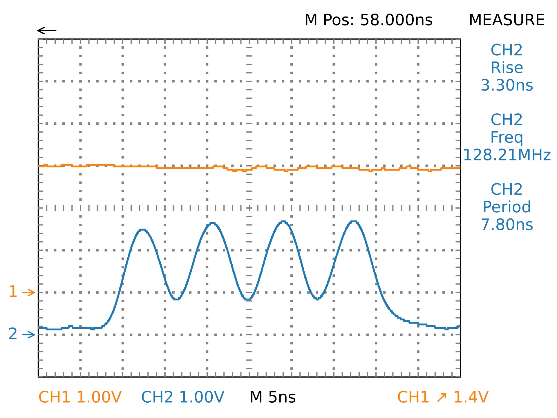
The number of pulses in the pulse train is limited to 4, 8, or 16. Note that time is needed to reload the DMA after each burst, the reloading time depends on the burst settings. In this example, it's 50 ns.
static void dma_config(void)
{
/*
* Select GPIO bank B as the source of the EXTI input line 0.
* GPIOB Pin 0 would generate a signal on EXTI Line 0.
*/
LL_SYSCFG_SetEXTISource(LL_SYSCFG_EXTI_PORTB, LL_SYSCFG_EXTI_LINE0);
/* Use EXTI Line 0 input's rising edge to trigger an IRQ. */
static LL_EXTI_InitTypeDef exti_ctx = {
.Line_0_31 = LL_EXTI_LINE_0,
.Line_32_63 = LL_EXTI_LINE_NONE,
.Line_64_95 = LL_EXTI_LINE_NONE,
.LineCommand = ENABLE,
.Mode = LL_EXTI_MODE_IT,
.Trigger = LL_EXTI_TRIGGER_RISING,
};
LL_EXTI_Init(&exti_ctx);
LL_AHB1_GRP1_EnableClock(LL_AHB1_GRP1_PERIPH_DMA1);
/* Use EXTI line 0's rising edge to generate DMA Request 0 */
LL_DMAMUX_SetRequestSignalID(
DMAMUX1, LL_DMAMUX_REQ_GEN_0, LL_DMAMUX1_REQ_GEN_EXTI0
);
LL_DMAMUX_SetRequestGenPolarity(
DMAMUX1, LL_DMAMUX_REQ_GEN_0, LL_DMAMUX_REQ_GEN_POL_RISING
);
LL_DMAMUX_SetGenRequestNb(DMAMUX1, LL_DMAMUX_REQ_GEN_0, 2);
LL_DMAMUX_EnableRequestGen(DMAMUX1, LL_DMAMUX_REQ_GEN_0);
__attribute__((section (".sram1_data")))
static const uint16_t gpio_data[] = {
0xFFFF, 0x0000, 0xFFFF, 0x0000,
};
static LL_DMA_InitTypeDef dma_ctx = {
.PeriphOrM2MSrcAddress = (uint32_t) &GPIOD->ODR,
.MemoryOrM2MDstAddress = (uint32_t) &gpio_data,
.Direction = LL_DMA_DIRECTION_MEMORY_TO_PERIPH,
.Mode = LL_DMA_MODE_CIRCULAR,
.PeriphOrM2MSrcIncMode = LL_DMA_PERIPH_NOINCREMENT,
.MemoryOrM2MDstIncMode = LL_DMA_MEMORY_INCREMENT,
.PeriphOrM2MSrcDataSize = LL_DMA_PDATAALIGN_HALFWORD,
.MemoryOrM2MDstDataSize = LL_DMA_MDATAALIGN_HALFWORD,
.NbData = sizeof(gpio_data) / sizeof(gpio_data[0]),
.PeriphRequest = LL_DMAMUX1_REQ_GENERATOR0,
.Priority = LL_DMA_PRIORITY_VERYHIGH,
.FIFOMode = LL_DMA_FIFOMODE_ENABLE,
.FIFOThreshold = LL_DMA_FIFOTHRESHOLD_FULL,
.MemBurst = LL_DMA_MBURST_INC8,
.PeriphBurst = LL_DMA_PBURST_INC8,
.DoubleBufferMode = LL_DMA_DOUBLEBUFFER_MODE_DISABLE,
/* don't care */
.TargetMemInDoubleBufferMode = LL_DMA_CURRENTTARGETMEM0,
};
LL_DMA_Init(DMA1, LL_DMA_STREAM_0, &dma_ctx);
LL_DMA_EnableStream(DMA1, LL_DMA_STREAM_0);
}Just make sure gpio_data is located in SRAM 1 (0x30000000) for DMA1, or SRAM 4 (0x38000000) for BDMA, may require custom startup and linker code. How to implement this is out of scope of this thread. I'm using a bare-metal environment, your mileage may vary.
What I do at startup:
void flash_to_mem(
char *flash_start,
volatile char *mem_start,
volatile char *mem_end
)
{
size_t len = mem_end - mem_start;
#ifdef SEMIHOSTING
printf(
"relocate %p-%p to %p, %d bytes\n",
flash_start,
flash_start + len,
mem_start,
len
);
#endif
/*
* Language Lawyering.
*
* Don't use memcpy(). This is widely used in embedded libraries, but it's
* a theoretical Undefined Behavior as C compilers can remove memcpy()
* when they don't have any visible effects to C code under the "as-if"
* rule. Mark destination variables as "volatile char *", and copy manual-
* ly. Keyword "volatile" ensures it's always executed, and "char *" is
* the only data type in C that is safe to cast into without breaking
* aliasing or alignment rules (even "uint8_t *" does not enjoy this
* exception).
*/
for (size_t i = 0; i < len; i++) {
mem_start[i] = flash_start[i];
}
}
void relocate_to_itcm(void)
{
extern char _si_isr_vector;
extern volatile char __isr_vector_start, __isr_vector_end;
flash_to_mem(&_si_isr_vector, &__isr_vector_start, &__isr_vector_end);
extern char _si_itcm_text;
extern volatile char __itcm_text_start, __itcm_text_end;
flash_to_mem(&_si_itcm_text, &__itcm_text_start, &__itcm_text_end);
SCB->VTOR = D1_ITCMRAM_BASE;
/*
* Test memory access latency by declaring arrays with:
*
* __attribute__((section (".axisram_data")))
* __attribute__((section (".sram1_data")))
* __attribute__((section (".sram2_data")))
* __attribute__((section (".sram3_data")))
* __attribute__((section (".sram4_data")))
*
* Note that different SRAMs have different access latency due
* to their bus locations. Some peripherals can only read from
* a specific SRAM bank (e.g. BDMA can only read from SRAM4).
*
* Not used in this example, can be removed.
*/
extern char _si_axisram_data;
extern volatile char __axisram_data_start, __axisram_data_end;
LL_AHB3_GRP1_EnableClock(LL_AHB3_GRP1_PERIPH_AXISRAM);
flash_to_mem(
&_si_axisram_data, &__axisram_data_start, &__axisram_data_end
);
extern char _si_sram1_data;
extern volatile char __sram1_data_start, __sram1_data_end;
LL_AHB2_GRP1_EnableClock(LL_AHB2_GRP1_PERIPH_D2SRAM1);
flash_to_mem(&_si_sram1_data, &__sram1_data_start, &__sram1_data_end);
extern char _si_sram2_data;
extern volatile char __sram2_data_start, __sram2_data_end;
LL_AHB2_GRP1_EnableClock(LL_AHB2_GRP1_PERIPH_D2SRAM2);
flash_to_mem(&_si_sram2_data, &__sram2_data_start, &__sram2_data_end);
extern char _si_sram3_data;
extern volatile char __sram3_data_start, __sram3_data_end;
LL_AHB2_GRP1_EnableClock(LL_AHB2_GRP1_PERIPH_D2SRAM3);
flash_to_mem(&_si_sram3_data, &__sram3_data_start, &__sram3_data_end);
extern char _si_sram4_data;
extern volatile char __sram4_data_start, __sram4_data_end;
LL_AHB4_GRP1_EnableClock(LL_AHB4_GRP1_PERIPH_SRAM4);
flash_to_mem(&_si_sram4_data, &__sram4_data_start, &__sram4_data_end);
}Using the following linker file:
/* SPDX-License-Identifier: Apache-2.0 AND (0BSD OR CC0-1.0) */
/*
******************************************************************************
**
** File : LinkerScript.ld
**
**
** Abstract : Linker script for STM32H7 series
** 2048Kbytes FLASH, 64Kbytes ITCMRAM, 128Kbytes DTCMRAM
**
** Set heap size, stack size and stack location according
** to application requirements.
**
** Set memory bank area and size if external memory is used.
**
** Target : STMicroelectronics STM32
**
** Distribution: The file is distributed as is without any warranty
** of any kind.
**
*****************************************************************************
** @attention
**
** Copyright (C) 2026 niconiconi.
**
** Modified from stm32h745xx_flash_CM7.ld to stm32h743xx_flash_CM7.ld,
** for STM32H7 support, including project-specific ITCM/DTCM customizations.
**
** This file is free software: you may copy, redistribute and/or modify it
** under the terms of the BSD Zero Clause License, or (at your option)
** Creative Commons Zero v1.0 Universal license. See "SPDX-License-Identifier"
** for more details.
**
** This file is distributed in the hope that it will be useful, but WITHOUT ANY
** WARRANTY; without even the implied warranty of MERCHANTABILITY or FITNESS
** FOR A PARTICULAR PURPOSE.
**
** This file incorporates work covered by the following copyright and
** permission notice:
**
** Copyright (c) 2019 STMicroelectronics.
** All rights reserved.
**
** This software is licensed under terms that can be found in the LICENSE
** file in the root directory of this software component. If no LICENSE
** file comes with this software, it is provided AS-IS.
**
** LICENSE file in the root directory of the origin:
**
** Component: CMSIS Device
** Copyright: ARM Limited, STMicroelectronics
** License: Apache License 2.0
**
******************************************************************************
*/
/* Entry Point */
ENTRY(Reset_Handler)
/* Highest address of the user mode stack */
_estack = 0x20020000; /* end of RAM */
/* Generate a link error if heap and stack don't fit into RAM */
_Min_Heap_Size = 0x200; /* required amount of heap */
_Min_Stack_Size = 0x400; /* required amount of stack */
/* Specify the memory areas */
MEMORY
{
FLASH (rx) : ORIGIN = 0x08000000, LENGTH = 2048K
ITCMRAM (xrw) : ORIGIN = 0x00000000, LENGTH = 64K
DTCMRAM (xrw) : ORIGIN = 0x20000000, LENGTH = 128K
AXISRAM (rw) : ORIGIN = 0x24000000, LENGTH = 512K
SRAM1 (rw) : ORIGIN = 0x30000000, LENGTH = 128K
SRAM2 (rw) : ORIGIN = 0x30020000, LENGTH = 128K
SRAM3 (rw) : ORIGIN = 0x30040000, LENGTH = 32K
SRAM4 (rw) : ORIGIN = 0x38000000, LENGTH = 64K
}
/* Define output sections */
SECTIONS
{
/* The startup code goes into ITCM (relocated from FLASH) */
.isr_vector :
{
. = ALIGN(4);
__isr_vector_start = .;
KEEP(*(.isr_vector)) /* Startup code */
. = ALIGN(4);
__isr_vector_end = .;
} >ITCMRAM AT> FLASH
.itcm_text :
{
. = ALIGN(4);
__itcm_text_start = .;
*(.itcm_text)
*(.itcm_text*)
. = ALIGN(4);
__itcm_text_end = .;
} > ITCMRAM AT> FLASH
/* used by the startup to initialize data */
_si_isr_vector = LOADADDR(.isr_vector);
_si_itcm_text = LOADADDR(".itcm_text");
/* The program code and other data goes into FLASH */
.text :
{
. = ALIGN(4);
*(.text) /* .text sections (code) */
*(.text*) /* .text* sections (code) */
*(.glue_7) /* glue arm to thumb code */
*(.glue_7t) /* glue thumb to arm code */
*(.eh_frame)
KEEP (*(.init))
KEEP (*(.fini))
. = ALIGN(4);
_etext = .; /* define a global symbols at end of code */
} >FLASH
/* Constant data goes into FLASH */
.rodata :
{
. = ALIGN(4);
*(.rodata) /* .rodata sections (constants, strings, etc.) */
*(.rodata*) /* .rodata* sections (constants, strings, etc.) */
. = ALIGN(4);
} >FLASH
.ARM.extab (READONLY) : /* The READONLY keyword is only supported in GCC11 and later, remove it if using GCC10 or earlier. */
{
. = ALIGN(4);
*(.ARM.extab* .gnu.linkonce.armextab.*)
. = ALIGN(4);
} >FLASH
.ARM (READONLY) : /* The READONLY keyword is only supported in GCC11 and later, remove it if using GCC10 or earlier. */
{
. = ALIGN(4);
__exidx_start = .;
*(.ARM.exidx*)
__exidx_end = .;
. = ALIGN(4);
} >FLASH
.preinit_array (READONLY) : /* The READONLY keyword is only supported in GCC11 and later, remove it if using GCC10 or earlier. */
{
. = ALIGN(4);
PROVIDE_HIDDEN (__preinit_array_start = .);
KEEP (*(.preinit_array*))
PROVIDE_HIDDEN (__preinit_array_end = .);
. = ALIGN(4);
} >FLASH
.init_array (READONLY) : /* The READONLY keyword is only supported in GCC11 and later, remove it if using GCC10 or earlier. */
{
. = ALIGN(4);
PROVIDE_HIDDEN (__init_array_start = .);
KEEP (*(SORT(.init_array.*)))
KEEP (*(.init_array*))
PROVIDE_HIDDEN (__init_array_end = .);
. = ALIGN(4);
} >FLASH
.fini_array (READONLY) : /* The READONLY keyword is only supported in GCC11 and later, remove it if using GCC10 or earlier. */
{
. = ALIGN(4);
PROVIDE_HIDDEN (__fini_array_start = .);
KEEP (*(SORT(.fini_array.*)))
KEEP (*(.fini_array*))
PROVIDE_HIDDEN (__fini_array_end = .);
. = ALIGN(4);
} >FLASH
/* used by the startup to initialize data */
_sidata = LOADADDR(.data);
_si_sram1_data = LOADADDR(.sram1_data);
_si_sram2_data = LOADADDR(.sram2_data);
_si_sram3_data = LOADADDR(.sram3_data);
_si_sram4_data = LOADADDR(.sram4_data);
_si_axisram_data = LOADADDR(.axisram_data);
/* Initialized data sections goes into RAM, load LMA copy after code */
.data :
{
. = ALIGN(4);
_sdata = .; /* create a global symbol at data start */
*(.data) /* .data sections */
*(.data*) /* .data* sections */
. = ALIGN(4);
_edata = .; /* define a global symbol at data end */
} >DTCMRAM AT> FLASH
.axisram_data :
{
. = ALIGN(4);
__axisram_data_start = .;
*(.axisram_data)
*(.axisram_data*)
. = ALIGN(4);
__axisram_data_end = .;
} >AXISRAM AT> FLASH
.sram1_data :
{
. = ALIGN(4);
__sram1_data_start = .;
*(.sram1_data)
*(.sram1_data*)
. = ALIGN(4);
__sram1_data_end = .;
} >SRAM1 AT> FLASH
.sram2_data :
{
. = ALIGN(4);
__sram2_data_start = .;
*(.sram2_data)
*(.sram2_data*)
. = ALIGN(4);
__sram2_data_end = .;
} >SRAM2 AT> FLASH
.sram3_data :
{
. = ALIGN(4);
__sram3_data_start = .;
*(.sram3_data)
*(.sram3_data*)
. = ALIGN(4);
__sram3_data_end = .;
} >SRAM3 AT> FLASH
.sram4_data :
{
. = ALIGN(4);
__sram4_data_start = .;
*(.sram4_data)
*(.sram4_data*)
. = ALIGN(4);
__sram4_data_end = .;
} >SRAM4 AT> FLASH
/* Uninitialized data section */
. = ALIGN(4);
.bss :
{
/* This is used by the startup in order to initialize the .bss section */
_sbss = .; /* define a global symbol at bss start */
__bss_start__ = _sbss;
*(.bss)
*(.bss*)
*(COMMON)
. = ALIGN(4);
_ebss = .; /* define a global symbol at bss end */
__bss_end__ = _ebss;
} >DTCMRAM
/* User_heap_stack section, used to check that there is enough RAM left */
._user_heap_stack :
{
. = ALIGN(8);
PROVIDE ( end = . );
PROVIDE ( _end = . );
. = . + _Min_Heap_Size;
. = . + _Min_Stack_Size;
. = ALIGN(8);
} >DTCMRAM
/* Remove information from the standard libraries */
/DISCARD/ :
{
libc.a ( * )
libm.a ( * )
libgcc.a ( * )
}
.ARM.attributes 0 : { *(.ARM.attributes) }
}