Turn on suggestions
Auto-suggest helps you quickly narrow down your search results by suggesting possible matches as you type.
Showing results for
- STMicroelectronics Community
- STM32 MCUs
- STM32 MCUs Products
- Custom board Design using STM32F446RE and STM32F10...
Options
- Subscribe to RSS Feed
- Mark Topic as New
- Mark Topic as Read
- Float this Topic for Current User
- Bookmark
- Subscribe
- Mute
- Printer Friendly Page
Custom board Design using STM32F446RE and STM32F103CBT6
Options
- Mark as New
- Bookmark
- Subscribe
- Mute
- Subscribe to RSS Feed
- Permalink
- Email to a Friend
- Report Inappropriate Content
2023-06-28 9:15 PM
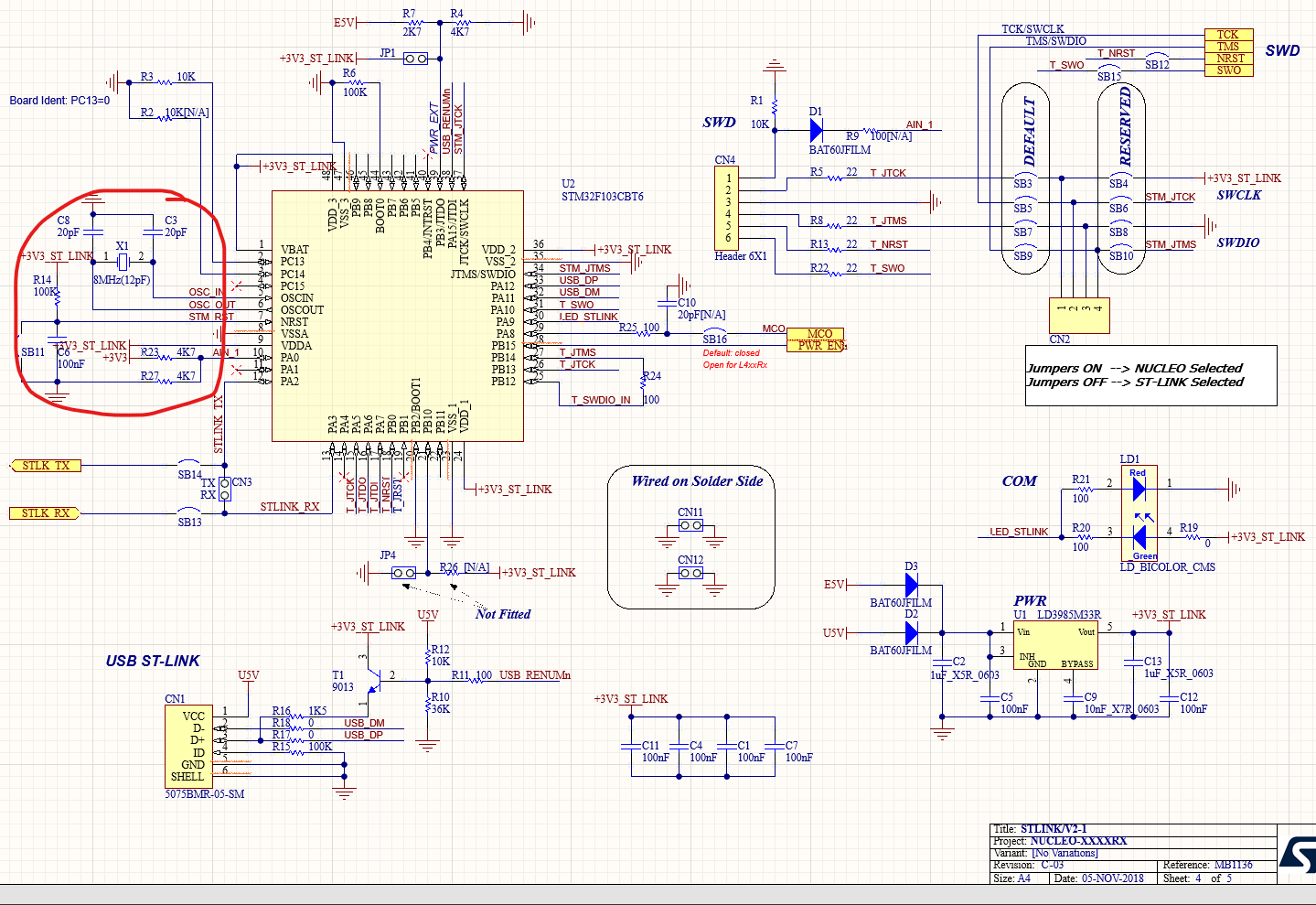
I am designing a custom board using STM32F446RE as main MCU and STM32F103CBT6 for ST link. I am using MB1136 board schematic as reference. I have the following questions:
1) Should I connect NRST of pin of main MCU to ST link MCU? But in reference schematic, I can't see both are connected together, instead on NRST pin of STM32F103CBT6 a capacitor and pullup resistor are connected. Please clarify the connection. I can't see any netlabel or port of same name for NRST. Please find attachment of reference design.
2) What is the use of PA0 pin. Why is it connected to +3V3 with two 4.7K resistor? Should I connect those when I design the custom board? Please clarify.
Thanks in advance
Labels:
- Labels:
-
STM32F1 Series
-
STM32F4 Series
This discussion is locked. Please start a new topic to ask your question.
1 REPLY 1
Options
- Mark as New
- Bookmark
- Subscribe
- Mute
- Subscribe to RSS Feed
- Permalink
- Email to a Friend
- Report Inappropriate Content
2023-06-29 8:53 AM
The ST-LINK firmware isn't open source so we can only make educated guesses here. If you're dead set on using the STM32F103 chip and making to a part of the board, I would copy the reference design exactly to future-proof yourself to firmware changes.
Looks like PA0 is being used as an ADC input to verify the ST_LINK +3V3 voltage.
Consider instead using the STLINK-V3MODS and soldering that directly to your board. That is the supported design direction. Or an external debugger.
https://www.st.com/en/development-tools/stlink-v3mods.html
If you feel a post has answered your question, please click "Accept as Solution".