- STMicroelectronics Community
- STM32 MCUs
- STM32 MCUs Products
- booting from bank 2 of STM32F4x9_eval
- Subscribe to RSS Feed
- Mark Topic as New
- Mark Topic as Read
- Float this Topic for Current User
- Bookmark
- Subscribe
- Mute
- Printer Friendly Page
booting from bank 2 of STM32F4x9_eval
- Mark as New
- Bookmark
- Subscribe
- Mute
- Subscribe to RSS Feed
- Permalink
- Email to a Friend
- Report Inappropriate Content
2013-10-24 10:44 AM
I run a program fine on bank 1. Then programmed BFB2 to 1. (BOOT0 = 0).
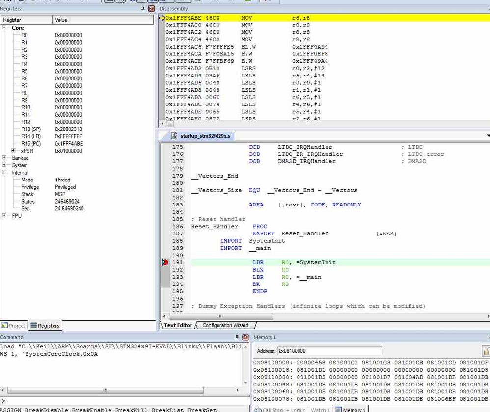
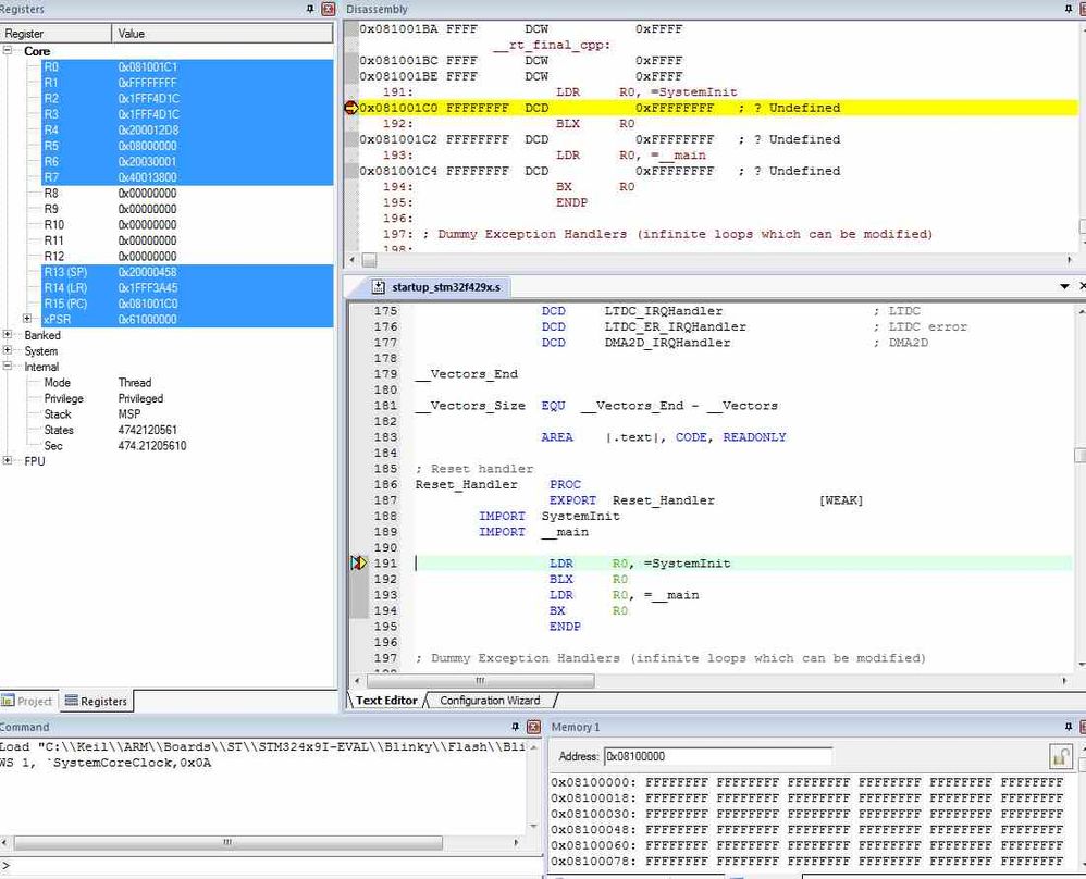
Compile Blinky to 0x08100000 and load it. Checked the flash by stlink-util and see0000: 20000468 081001c1.Those are correspondent to the .map file of STACK and reset_handler. Ok, good to go.Of course it won't work.I fired up the Keil debugger. found it began at 0x1fff 4abe, it's the bootloader. Fine, which is consistent to document. When BFB2 is 1, it will go to boot loader, then jump to bank 2.content on memory windows that shows normal too. then after a few steps (0x1fff4ac6). PC become 0x081001c0. all the flash contect become FF. I checked again the content by stlink. It's still valid, not FF. and of course. The PC is not the address of reset_handler.
  Somewhere in bootloader didn't go as I hope. (load SP from 0x08100000, and jump to 0x08100004 -> 0x081001c1 (reset_handle).). I wonder what's go wrong....The hardware is the STM32F4x9_EVAL.Sink
- Mark as New
- Bookmark
- Subscribe
- Mute
- Subscribe to RSS Feed
- Permalink
- Email to a Friend
- Report Inappropriate Content
2013-10-24 12:09 PM
Review the memory subsequently mapped at ZERO and 0x08000000
Up vote any posts that you find helpful, it shows what's working..
- Mark as New
- Bookmark
- Subscribe
- Mute
- Subscribe to RSS Feed
- Permalink
- Email to a Friend
- Report Inappropriate Content
2013-10-24 12:28 PM
- Mark as New
- Bookmark
- Subscribe
- Mute
- Subscribe to RSS Feed
- Permalink
- Email to a Friend
- Report Inappropriate Content
2013-10-24 12:49 PM
The hardware swaps Bank1 and Bank2 in the memory space, and can then map at zero.
Change your memory view window to 0x08000000 in the debuggerUp vote any posts that you find helpful, it shows what's working..
- Mark as New
- Bookmark
- Subscribe
- Mute
- Subscribe to RSS Feed
- Permalink
- Email to a Friend
- Report Inappropriate Content
2013-10-24 2:43 PM
I am stuck now. It seems that in order to boot from bank2. I need to build/link the program at 0x08000000, but load it to 0x08100000. So later when bootloader make the address swap. it can run correctly. Is that right?
When I tried to do that. I found neither Keil flash programmer nor STLink-util allow me to load hex file that build 0n 0x08000000 to 0x08100000. Is there application note document the dual boot mechanism beside AN2606? what's the correct/normal procedure?Regards,Sink- Mark as New
- Bookmark
- Subscribe
- Mute
- Subscribe to RSS Feed
- Permalink
- Email to a Friend
- Report Inappropriate Content
2013-10-24 3:31 PM
I'd supposed you'd compile/link for 0x08000000, and instead of using a .HEX, you get FromELF to make a .BIN file, which doesn't infer a load address, and then get the ST-LINK utilities to load the .BIN and program it at 0x08100000 from there (Start Address in Download dialog).
Up vote any posts that you find helpful, it shows what's working..
- Mark as New
- Bookmark
- Subscribe
- Mute
- Subscribe to RSS Feed
- Permalink
- Email to a Friend
- Report Inappropriate Content
2013-10-24 3:53 PM
I haven't at this juncture reviewed the App Note in question, I've been reviewing the Reference Manual and playing with the silicon. I played with the mapping register some time ago in terms of swapping the Flash Banks, and also the SDRAM.
Shadowing ROM files at different addresses, and compiling/loading files at assorted addresses is relatively straight forward from a Boot Loader perspective. I haven't spent a lot of time pondering how I might get Keil to program to the high bank, but I suppose it could be done with an INI script to program the bank mapping registers, or customizing the Flash Applet. Programming the upper bank seems more of a production exercise than a debugging one, and part of the job of the boot loader. Certainly from the perspective of programming, upgrading and managing alternate application images.I'd probably tend more toward keeping a 16KB boot loader, and staging an update in the upper bank, rather than ping-pong between the two, although I can see the advantage of being able to regress. That said most of the interest has been in getting ~2MB of app space, and staging updates on an SD Card, or running larger apps from SDRAM.Up vote any posts that you find helpful, it shows what's working..
- Mark as New
- Bookmark
- Subscribe
- Mute
- Subscribe to RSS Feed
- Permalink
- Email to a Friend
- Report Inappropriate Content
2013-10-24 4:18 PM
Took a look at the
http://www.st.com/web/en/resource/technical/document/application_note/CD00167594.pdf
, does all seem rather contrived, kind of pushes off the responsibility of the Boot Loader to the System Loader. The sanity checking for the app doesn't seem to be very robust, basically checking if Stack resides above 0x20000000, as best I can tell. I'd rather it check the integrity of the whole image rather than a single page, or a couple of words at the front end. Flashing tends to write in a linear fashion so a write failure deeper into the image won't be caught.The prime benefits being not changing the mapping of running code, no app code changes, and how the address swapping is handled by ARTUp vote any posts that you find helpful, it shows what's working..
- Mark as New
- Bookmark
- Subscribe
- Mute
- Subscribe to RSS Feed
- Permalink
- Email to a Friend
- Report Inappropriate Content
2013-10-24 4:28 PM
Yeah, currently I convert .hex to .bin then program to high bank to achieve the dual bank booting of the system that require golden/current image operation.
I tried to set up .sct file like LR_IROM1 0x08100000 0x00100000 { ; load region size_region ER_IROM1 0x00000000 0x00100000 { ; execution address *.o (RESET, +First) *(InRoot$$Sections) .ANY (+RO) } RW_IRAM1 0x20000000 0x00030000 { ; RW data .ANY (+RW +ZI) }}to see if I can make Keil to work as I want. But then I got'cannot be assigned to non-root region' error. so I didn't find 'simple way' to do high bank linking/flashing yet. Sink.- Mark as New
- Bookmark
- Subscribe
- Mute
- Subscribe to RSS Feed
- Permalink
- Email to a Friend
- Report Inappropriate Content
2018-06-14 8:59 AM
Hi Sink
We are facing the same problemMyapproach
to achieve 'high bank linking/flashing'
is followed:1) Flash the program to bank1 (as usuall, when no bootloading is considered)2) The program contains a function, that when triggered, copies its own ontent to bank 2 (note that bank 2 need to be first erased by the same function, otherwise copying the code fails)3) Towards the end of the aforementioned function, The program checks for the value of BFB2. If it points to bank1, it toggles its value (HAL_FLASHEx_AdvOBProgram can be used)
4) Reset the device
In order to verify my approach works, another step should that corrupts bank1 is to be added.
Not sure it works 100% will update after some debugging and experimentation- STM32L496 errata (ES0335) Dual-bank boot - unable to reproduce in STM32 MCUs Products
- STM32F429IGT6 Dual Bank OTA updates in STM32 MCUs Wireless
- Dual Banking in stm32wle5ccu6 in STM32 MCUs Wireless
- STM32WB55 Error on start of BLE stack in STM32 MCUs Wireless
- Secure Boot STiROT with Dual Bank STM32H573 in STM32 MCUs Security