- STMicroelectronics Community
- STM32 MCUs
- STM32 MCUs Products
- ADC triger on PWM edge
- Subscribe to RSS Feed
- Mark Topic as New
- Mark Topic as Read
- Float this Topic for Current User
- Bookmark
- Subscribe
- Mute
- Printer Friendly Page
ADC triger on PWM edge
- Mark as New
- Bookmark
- Subscribe
- Mute
- Subscribe to RSS Feed
- Permalink
- Email to a Friend
- Report Inappropriate Content
2017-01-25 1:27 PM
Hello,
On a STM32F407VE device i have a timer2 which reads 3 hall sensors from a bldc motor, this timer is feeding the trigger signal into a advanced timer1 which generates 6pwm's for the transistor bridge.
The reading of the hall sensors and the comutation step configs, are made inside the timer2 cc1 irq handler.
The FET signals are TIM_OCMode_PWM1 for high side channels ( CH1, CH2,CH3) and for low side channel ( CH1N, CH2N, CH3N) its just regular low/high state
Till here everything is ok, the signals have the corect phase
But i was thinking to ad a current measurement feature using one ADC channel ( ADC_Channel_14 on PC4 pin) which reads a shunt resistor between low side FET's and ground(GND).
Since i use pwm I was wondering if there is any method using ADC to sync the aquisition trigger on the 'on state' of the pwm signals?
Do i need DMA for this? since i work only with one physical adc channel
What is.. lets say common practice to configure ADC to capture in sync with pwm 'on time'? Maybe a code reference would be also fit well.
Thank you
- Mark as New
- Bookmark
- Subscribe
- Mute
- Subscribe to RSS Feed
- Permalink
- Email to a Friend
- Report Inappropriate Content
2017-01-25 1:48 PM
TIM1_CH1/CH2/CH3 can trigger regular conversions, TIM1_CH4 and TIM1_TRGO (which can be set to any channel's compare output) can trigger injected conversions. See Figure 44 in RM0090 rev.13.
JW
- Mark as New
- Bookmark
- Subscribe
- Mute
- Subscribe to RSS Feed
- Permalink
- Email to a Friend
- Report Inappropriate Content
2017-01-25 10:54 PM
Hello,
thank you for the information... i have done the following code for ADC initialization
ADC_StructInit(&ADC_InitStructure);
ADC_CommonStructInit(&ADC_CommonInitStructure);ADC_Cmd(ADC1, DISABLE);ADC_DeInit();NVIC_InitStructure.NVIC_IRQChannel = ADC_IRQn;
NVIC_InitStructure.NVIC_IRQChannelPreemptionPriority = 4; NVIC_InitStructure.NVIC_IRQChannelSubPriority = 4; NVIC_InitStructure.NVIC_IRQChannelCmd = ENABLE; NVIC_Init(&NVIC_InitStructure); ADC_CommonInitStructure.ADC_Mode = ADC_Mode_Independent; ADC_CommonInitStructure.ADC_Prescaler = ADC_Prescaler_Div2; ADC_CommonInitStructure.ADC_DMAAccessMode = ADC_DMAAccessMode_Disabled; ADC_CommonInitStructure.ADC_TwoSamplingDelay = ADC_TwoSamplingDelay_5Cycles; ADC_CommonInit(&ADC_CommonInitStructure);ADC_InitStructure.ADC_Resolution = ADC_Resolution_12b;
ADC_InitStructure.ADC_ScanConvMode = ENABLE; ADC_InitStructure.ADC_ContinuousConvMode = DISABLE; ADC_InitStructure.ADC_ExternalTrigConvEdge = ADC_ExternalTrigConvEdge_Rising; ADC_InitStructure.ADC_ExternalTrigConv = ADC_ExternalTrigConv_T1_TRGO; // external trigger from timer1 TRGO ADC_InitStructure.ADC_DataAlign = ADC_DataAlign_Right; ADC_InitStructure.ADC_NbrOfConversion = 1; // 1 channel in total ADC_Init(ADC1, &ADC_InitStructure); ADC_TempSensorVrefintCmd(ENABLE); ADC_InjectedSequencerLengthConfig(ADC1, 0);// Set injected sequencer length ADC_InjectedChannelConfig(ADC1, ADC_Channel_14, 1, ADC_SampleTime_3Cycles); ADC_ExternalTrigInjectedConvConfig(ADC1, ADC_ExternalTrigInjecConv_T1_TRGO); // ADC_ExternalTrigInjectedConvCmd(ADC1, ENABLE); ADC_AutoInjectedConvCmd(ADC1, ENABLE); ADC_ITConfig(ADC1, ADC_IT_JEOC, ENABLE);// Enable injected end of conversion interrupt ADC_Cmd(ADC1, ENABLE); // enable adcAnd bellow is the ADC IRQ Handler using the JEOC IT
void ADC_IRQHandler(void){
if(ADC_GetITStatus(ADC1,ADC_IT_JEOC)){ // end of conversion event
GPIO_ToggleBits(GPIOC, GPIO_Pin_15); // toggle for trace on logic analyzer GPIO_ToggleBits(GPIOC, GPIO_Pin_15);// toggle for trace on logic analyzer
value=ADC_GetInjectedConversionValue(ADC1, ADC_InjectedChannel_1);
ADC_ClearITPendingBit(ADC1, ADC_IT_JEOC);// Clear ADC1 JEOC pending interrupt bit }On the logic analyzer i can see its toggles , but i tryied to read and convert the value in voltage, and i get 3.2v, 2.6V, and 0.2V ...
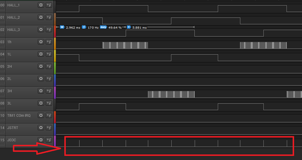
As seen this on the logic capture, i fear that the adc is trigerd at every hall event, and not at the midle of a pwm ''on cycle''. How to overcome this?
Since i am not familiar with usage of adc injecte mode, i fear i am doing something wrong

- STM32 + Freertos + Audio recording + FATFS. Audio really choppy and white noisy in STM32 MCUs Embedded software
- STM32H753 SPI6 Slave (H7 SPI v2) — Frame qualifies only with NSS-synchronised arming in STM32 MCUs Embedded software
- Access function for EXTI handle of a timer in STM32 MCUs Embedded software
- Experimenting with STM32 Clock Configuration Outside of CubeMX in Others: STM32 MCUs related
- STM32G4: trigger one DMA stream by both capture & overflow/update timer events? in STM32 MCUs Products