- STMicroelectronics Community
- STM32 MCUs
- STM32 MCUs Boards and hardware tools
- Moving from STM32F4-Discovery to a custom board - ...
- Subscribe to RSS Feed
- Mark Topic as New
- Mark Topic as Read
- Float this Topic for Current User
- Bookmark
- Subscribe
- Mute
- Printer Friendly Page
Moving from STM32F4-Discovery to a custom board - Checklist and Final Review...
- Mark as New
- Bookmark
- Subscribe
- Mute
- Subscribe to RSS Feed
- Permalink
- Email to a Friend
- Report Inappropriate Content
2019-01-30 4:16 PM
As I'm now done with the development of the main firmware for my product and ready to move my design to a custom board, I thought it might be worthwhile to make a checklist of the most important things to be considered by the designer in order to avoid confusion and troubles at a late stage of the production.
I will divide this into several sections:
1- Bootloader settings, pins, and DFU
I have read AN2606 (STM32 microcontroller system memory boot mode) I can connect to device and program it over USART (booting from system memory) but it's not the case for DFU. For some reason, DfuSe REFUSEs to detect the board, but Windows detects and enumerates the device as "STM32 Bootloader". ON the STM32 Cube Programmer, I was able to connect the device, perform erase, but the connection is lost before erase finishes. Tried it many times but had the same issue. I have modified the USB circuit on the board for testing purposes so I'm not sure if that could make any difference. Yet to be tested and reported later.
2- USB Device circuit
I started by reading AN4879 (USB hardware and PCB guidelines using STM32 MCUs).
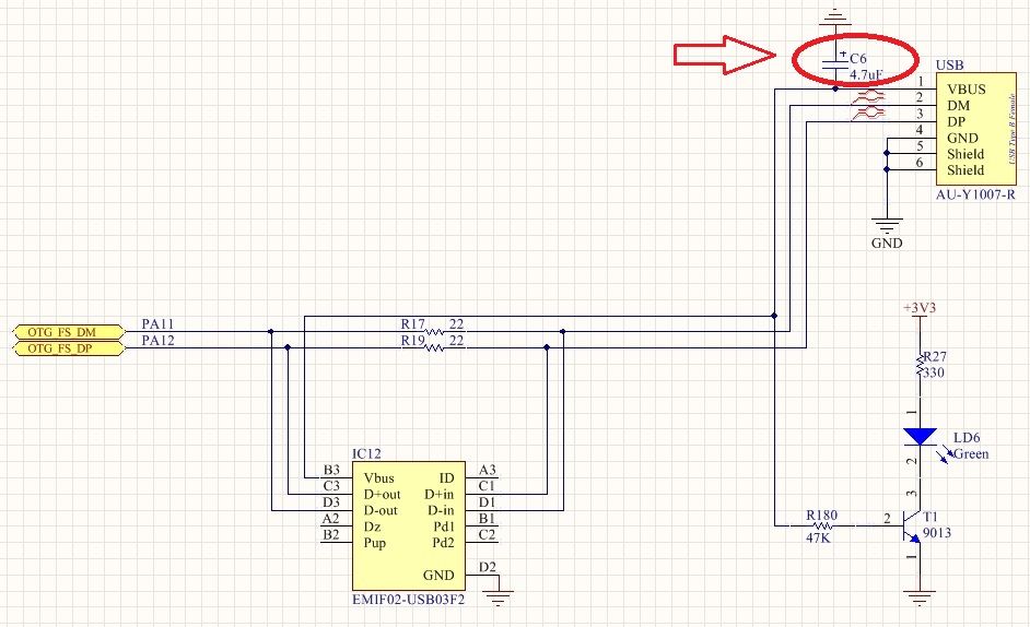
I will need USB in device-mode only for MSC, no host, so I have disabled the VBUS sensing, ID signal, and removed U6 (STMPS2141STR) from the board so I can test if it affects the enumeration of the device on the host PC. Everything works fine, device is enumerated and I can access the storage medium (uSD card) read/write on the PC, however, the performance is terrible. It takes roughly 10 seconds to write 1.4 MBytes to the card over the USB connection. I don't know if there's any way to make it better. So, in my custom board, there won't be VBUS sensing, ID, as well as, overCurrent (STMPS2141STR). By the way, PD5 is used by the FSMC and LD8 always flashes during access to the external memory-mapped device. Since there's no use for these signals in my application, I assume it's safe to eliminate them altogether on my custom board. This is how the USB circuit looks like now:
I believe cap C6 is also not needed anymore since U6 is no longer there.
3- Power supply, bypass caps, and layout
I'm now studying AN4488 (Getting started with STM32F4xxxx MCU hardware development) and will write more if I have encountered any ambiguities.
4- Finally, protecting the firmware, OTA, SBSFU for stm32f407VGT6
Still need some time to understand what has been covered by UM2262 (Getting started with the X-CUBE-SBSFU) and AN5056 (Integration guide for the X-CUBE-SBSFU). But a quick question for now, is there any way to implement a dual-image FW upgrade on devices with single-bank flash (STM32F407)? I remember reading something about "remapping and definition" of certain flash regions for this purpose, but like I said earlier, I need to spend more time studying the material in order to get where I want.
I'm open to comments, suggestions, or any input that could help me avoid any issue before production of final board.
Thank you for your time!
Zaher
- Labels:
-
STM32F4 Series
