- STMicroelectronics Community
- MEMS and sensors
- MEMS (sensors)
- Hi there, We just realized we made an error in the...
- Subscribe to RSS Feed
- Mark Topic as New
- Mark Topic as Read
- Float this Topic for Current User
- Bookmark
- Subscribe
- Mute
- Printer Friendly Page
Hi there,
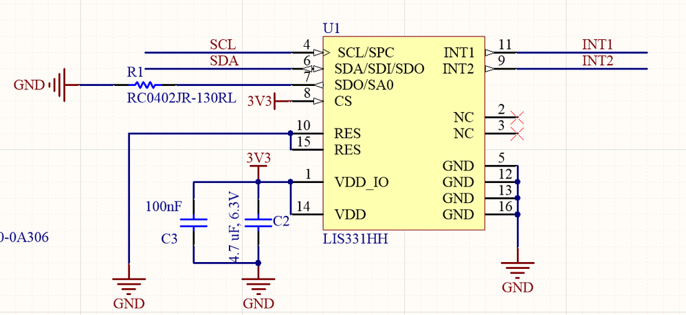
We just realized we made an error in the schematic and we would like some advice from ST.
the LIS331 has 2 reserved pin (10 and 15), we erroneously have connected the pin 15 to GND. would this stop the LIS331 to work?
Thank you,
Francesco
- Mark as New
- Bookmark
- Subscribe
- Mute
- Subscribe to RSS Feed
- Permalink
- Email to a Friend
- Report Inappropriate Content
2020-09-26 4:32 AM
Accepted Solutions
- Mark as New
- Bookmark
- Subscribe
- Mute
- Subscribe to RSS Feed
- Permalink
- Email to a Friend
- Report Inappropriate Content
2020-09-29 3:18 AM
Hi @FPode.1 ,
I unfortunately don't have good news about your question... the PIN 15 is used for programming and erasing the internal flash memory, since the HV levels needed for this purpose are generated using this supply. From internal check, I can say you that it is mandatory to keep the pad level over 1.8V in any functional mode. Max voltage on this supply is 13.5V. When not used for programming purpose this pad must be kept to power supply (VDD).
If you could invert the polarity of the reserved pins, i.e. both PIN10 and PIN15 to VDD level, things may be more safe for a standard working mode of the device...
-Eleon
- Mark as New
- Bookmark
- Subscribe
- Mute
- Subscribe to RSS Feed
- Permalink
- Email to a Friend
- Report Inappropriate Content
2020-09-28 3:28 AM
Hello,
can anyone from ST answer the question?
We acknowledge that we made an error, we are trying to understand if we can use the PCB that we have just received.
Thank you!
Francesco
- Mark as New
- Bookmark
- Subscribe
- Mute
- Subscribe to RSS Feed
- Permalink
- Email to a Friend
- Report Inappropriate Content
2020-09-29 3:18 AM
Hi @FPode.1 ,
I unfortunately don't have good news about your question... the PIN 15 is used for programming and erasing the internal flash memory, since the HV levels needed for this purpose are generated using this supply. From internal check, I can say you that it is mandatory to keep the pad level over 1.8V in any functional mode. Max voltage on this supply is 13.5V. When not used for programming purpose this pad must be kept to power supply (VDD).
If you could invert the polarity of the reserved pins, i.e. both PIN10 and PIN15 to VDD level, things may be more safe for a standard working mode of the device...
-Eleon
- Mark as New
- Bookmark
- Subscribe
- Mute
- Subscribe to RSS Feed
- Permalink
- Email to a Friend
- Report Inappropriate Content
2020-09-29 3:22 AM
Hi Eleon,
thank you for your time...
We will fix and respin the PCB.
Kind regards,
Francesco
