- STMicroelectronics Community
- Knowledge base
- MEMS and sensors
- How to optimize your PCB design for MEMS sensors
- Subscribe to RSS Feed
- Mark as New
- Mark as Read
- Bookmark
- Subscribe
- Email to a Friend
- Printer Friendly Page
- Report Inappropriate Content
How to optimize your PCB design for MEMS sensors
- Subscribe to RSS Feed
- Mark as New
- Mark as Read
- Bookmark
- Subscribe
- Email to a Friend
- Printer Friendly Page
- Report Inappropriate Content
on 2023-11-14 7:31 AM
Summary
This article provides the basic rules to be followed to ensure an optimal PCB design based on STMicroelectronics MEMS technology.
The reference for the layout guidelines is the technical note TN0018 available from st.com.
“Do” and “don’t” recommendations that designers have to consider during the PCB design are also described.
1. Effects of thermomechanical stress
1.1. Soldering effect on the MEMS
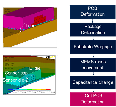
Assembly processes can induce thermomechanical stress to the sensor due to the interaction between the sensor die, package, and PCB.
Basically, the deformation of the PCB is transferred to the substrate and to the package of the sensor. Then the mechanical stress is transferred to the mechanical structure of the sensor through its anchors. This causes a deviation/drift of sensor parameters, such as offset, sensitivity, and self-test response. In the worst case, aggressive handling may lead to breakage of the structures of the sensor.

1.2. Effect of thermomechanical offset drift on the sensor
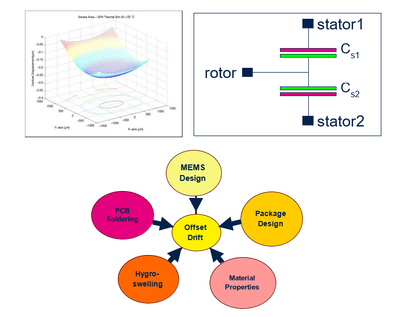
Thermomechanical stress causes a deformation of the silicon die of the sensor, which is converted into a relative displacement between the fixed and movable electrodes. For the sensors, this displacement produces a signal comparable to a real physical one. This produces, for example, a variation of the offset of the device.
The actual variation of the sensor parameters related to thermomechanical offset drift depends on several variables (package, materials, MEMS design, soldering process, etc).

1.3. Effect of thermomechanical stress: elastic vs. plastic
Thermomechanical stress, and related warpage, always happen when there are changes in temperature:
Thermomechanical stress, and related warpage, always happen when there are changes in temperature:
- It is usually an elastic effect
- When the external force is removed, the warpage is relaxed
- Package materials have been selected and the sensor has been designed to minimize this effect.
- During soldering some plastic deformation can happen in the package due to:
- Interaction with the PCB, uneven force field
- Process not optimized, for example, temperature ramp down in reflow oven. Plastic deformation does not relax back when the temperature stress is removed
1.4. Mechanical stress factors
Uneven force field distribution is created by:
- Asymmetrical PCB layout, surrounding components, position of the vias
- Placement of MEMS component
- Usage and dispensing of filler
- Nonuniformity of solder paste thickness
Other factors to be considered for optimized performance are:
- Very thick solder paste reduces the level of warpage of the sensor
- Slow cooling of the board after assembly (JEDEC specs) is recommended to avoid stress on the sensor
- It is recommended to avoid g-forces exceeding the specified sensor limits during all handling operations, including transportation and assembly
2. Importance of a good layout
2.1. PCB design rules for the footprint
Footprint design rules are taken from technical note TN0018. Note that all lands have to be the same size, no need for large lands.

2.2. PCB design rules for the traces
Connecting traces should be designed symmetrically.
All traces should flow outside the component, parallel to the long edge of the pad.
The traces must have the same thickness. There is no need to have thicker traces for power signals since very low current can flow into them. This is to avoid potential mechanical stress.
The ground plane should not be connected directly to the footprint pads. It is better to connect it through a standard trace.

2.3. Placement rules for the top side
For all MEMS devices, the device is soldered on the top side.
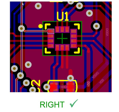
Never place any routing or via on the top side under the device, refer to the following figure.

2.4. Placement rules for the bottom side
Placement rules for the bottom side apply only to MEMS accelerometer, gyroscope, and pressure sensors. It is possible to use the bottom side under the device for power plane or signal routing.

2.5. LGA package layout hints - extra tips
The following figure shows an actual case from the field.
The customer was facing a little offset shift on the zero-g and zero-rate level. The following points were identified as incorrect practices:
- Pins 6 and 7 are not soldered: this can cause mechanical stress on the inner sensors.
- Vias below pads: it is better to move these outside the component.
- Copper traces below the component have to be avoided (trace of pin 8 should flow directly outside the component).

3. Placement considerations for inertial MEMS sensors on the PCB
3.1. Mechanical stress and layout tips
Thermomechanical stress is a normal process during component assembly and the effect is fully recovered once the stress conditions return to normal. In fact, even if the layout is symmetrical, PCB, and solder joints need time to relax the induced stress.
On the other hand, permanent unexpected levels of sensor output can be caused by a anisotropic mechanical stress distribution on the PCB. This is typically generated by:
- Screw, holes, pillars
- Shields placed in close proximity to the device
- Underfill (when placed close /on the opposite side of the MEMS)
Moreover, to prevent high temperature gradients that could cause mechanical stress, STMicroelectronicsMicroelectronics recommends placing the sensor away from heat sources (such as batteries and power management integrated circuits).
All these elements should be carefully evaluated during PCB design.
3.2. Fasteners on the PCB
PCB boards are generally housed and fixed in an enclosure. Inertial MEMS sensors should be located between fasteners so as to minimize and distribute homogenously the stress on the MEMS sensor. This is illustrated in the following figure. When this is not possible, the location, which best meets this criteria is to be selected.

3.3. Areas of stress on the PCB
The PCB board illustrated in the previous figure is a symmetric rectangular board. In real life applications, the probability of having a symmetric board is unlikely. In most cases, PCBs have protruding sections and without fasteners. These locations are prone to vibrations, which can provide false readouts and thus it is highly advisable that the MEMS sensor be located away from such areas.

Sources of stress can be the use of epoxy resin materials to cover the CPU. It can also be usage of heat sinks or other foreign structures, which are in contact with the MEMS sensors. These conditions are sources of high stress and need to be removed from the design.

3.4. Recommended placement of a heat source with respect to the MEMS sensor
The presence of a heat source in the surrounding area of the MEMS sensor causes undesired internal movement.
To reduce the probability of mechanical stress, locating the heat source away from the MEMS sensor is recommended.

3.5. External loads/forces
Certain applications allow the possibility for external loads/forces to be exerted on the board. One example might be a series of pushbuttons or connection points, which are used during normal operation.
These forces are transferred to the board and hence to the MEMS sensor. Placing the MEMS sensor away from these sources and keeping it at least 10 mm away from the source of the external force reduces the effect on the MEMS sensor.

Conclusion
This article provides PCB design guidelines for obtaining optimal performance from MEMS sensors, including solutions for thermomechanical stress, rules for PCB layout, as well as placement recommendations.
The reference for the layout guidelines is the technical note "Surface mounting guidelines for MEMS sensors in an LGA package" TN0018 available from st.com
You may be also interested in exploring the technical note "PCB design guidelines for MEMS sensors" TN1383 available from st.com
