- STMicroelectronics Community
- Knowledge base
- STM32 MCUs
- How to place and execute STM32 code in SRAM memory...
- Subscribe to RSS Feed
- Mark as New
- Mark as Read
- Bookmark
- Subscribe
- Email to a Friend
- Printer Friendly Page
- Report Inappropriate Content
How to place and execute STM32 code in SRAM memory with STM32CubeIDE
- Subscribe to RSS Feed
- Mark as New
- Mark as Read
- Bookmark
- Subscribe
- Email to a Friend
- Printer Friendly Page
- Report Inappropriate Content
on
2023-04-21
6:40 AM
- edited on
2025-10-23
7:28 AM
by
![]() Laurids_PETERSE
Laurids_PETERSE
This article aims to show some methods to set up STM32 project firmware to be able to execute a part or the entire firmware into embedded SRAM memory. Generally, STM32s execute user code directly from their embedded flash memory.
Thanks to the mechanism of ART Accelerator and Prefetch buffer that allows the execution of the code with a minimum flash wait state latency at a maximum cpu and peripheral frequency.
But in some cases, it is useful to execute a part or a full firmware in SRAM.
This can motivate an embedded system developer for the following reasons:
- Improve the execution times of code or interrupts considered critical.
- Reduce power consumption by placing the flash memory in low-power mode.
- Perform other concurrent read/write operations on flash memory, while the CPU is executing code in SRAM.
- Speed up the code upload when doing debugging sessions.
All the following examples use:
- NUCLEO-U575ZI-Q
- STM32CubeIDE and STM32Cube_FW_U5_V1.2.0
- STM32CubeProgrammer
Case 1: Placing and executing a function in SRAM
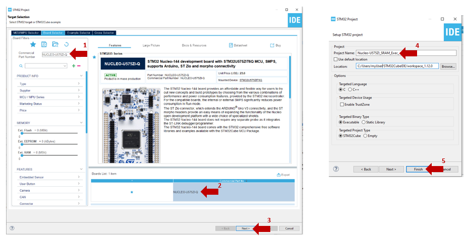
This part describes the steps to link and execute a C function in SRAM using STM32CubeIDE. In this example, we create a basic function called Prime_Calc_SRAM() in charge of computing an amount of Prime number in a given interval.
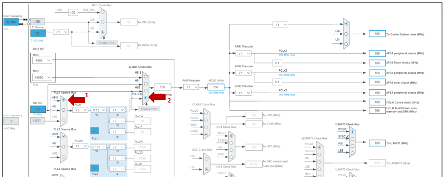
3. Leave all the STM32CubeMX configuration to the default value except:
- Clock configuration from MSI and PLL to obtain HCLK = 160 MHz
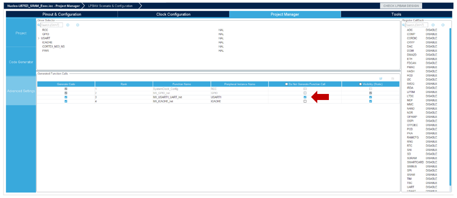
../Core/Src/main.c:382:13: warning: 'MX_USART1_UART_Init' defined but not used [-Wunused-function]
7. Open the main.c file and create the prototype of Prime_Calc_SRAM() function, which is in charge of computing the prime number in an array.
Note: This function is defined with __attribute__((section(".RamFunc"))) keyword.
/* USER CODE BEGIN PFP */
static void __attribute__((section(".RamFunc"))) Prime_Calc_SRAM(void);
/* USER CODE END PFP *//* USER CODE BEGIN PD */
#define PRIM_NUM 64U /* Size of the prime array */
/* USER CODE END PD */Note: This variable array is defined with __attribute__(( aligned(32))) keyword to make sure that the data as well is aligned into the memory.
/* USER CODE BEGIN PV */
static __attribute__(( aligned(32))) uint32_t primes_ram[PRIM_NUM];
/* USER CODE END PV */This code is in charge of computing the prime numbers from 2 to 311 (PRIM_NUM) and storing them into the primes_ram array variable.
It produces the prime numbers below and stores them in primes_ram array variable.
2, 3, 5, 7, 11, 13, 17, 19,
23, 29, 31, 37, 41, 43, 47, 53,
59, 61, 67, 71, 73, 79, 83, 89,
97, 101, 103, 107, 109, 113, 127,
131,137, 139, 149, 151, 157, 163, 167,
173, 179, 181, 191, 193, 197, 199, 211,
223, 227, 229, 233, 239, 241, 251, 257,
263, 269, 271, 277, 281, 283, 293, 307, 311
Note: As for the prototype definition the presence of the __attribute__(( aligned(32))) keyword.
/* USER CODE BEGIN 0 */

/**
  * @brief  Compute an amount of Prime number in SRAM
  *   None
  * @retval None
  */
static void __attribute__((section(".RamFunc"))) Prime_Calc_SRAM(void)
{
  /* Compute prime number in the elements size of the array */
  /* Initial condition */
  primes_ram[0] = 2;  // First prime number
  uint32_t count = 1; // Number of primes found
  uint32_t num = 3;   // Number to test for primality

  while (count < PRIM_NUM)
  {
    uint8_t is_prime = 1;
    for (uint32_t i = 0; i < count; i++)
    {
      if (num % primes_ram[i] == 0)
      {
        is_prime = 0;
        break;
      }
      if (primes_ram[i] * primes_ram[i] > num)
        break;
    }

    if (is_prime)
    {
      primes_ram[count] = num;
      count++;
    }
    num += 2; // Skip even numbers
  }
}
/* USER CODE END 0 *//* USER CODE BEGIN 2 */
Prime_Calc_SRAM();
/* USER CODE END 2 *//* Memories definition */
MEMORY
{
RAM (xrw) : ORIGIN = 0x20000000, LENGTH = 768K
SRAM4 (xrw) : ORIGIN = 0x28000000, LENGTH = 16K
FLASH (rx) : ORIGIN = 0x08000000, LENGTH = 2048K
} Refer to the STM32U5 reference manual (RM0456), chapter 2.3 "Memory organization" for a full description of the memory organization in the device.
Next, we can see the section dedicated for the interrupt vector (.isr_vector), placed by default at the beginning of the flash memory, then the program code (.text) also in flash memory and variable, bss heap, and stack in (.data, .bss, ._user_heap_stack) in RAM.
For us, our goal is to use a section placement that is defined in section .data, and it is named: .RamFunc - see below:
/* Initialized data sections into "RAM" Ram type memory */
.data :
{
  _sdata = .;        /* create a global symbol at data start */
  *(.data)           /* .data sections */
  *(.data*)          /* .data* sections */
  *(.RamFunc)        /* .RamFunc sections */
  *(.RamFunc*)       /* .RamFunc* sections */
  _edata = .;        /* define a global symbol at data end */
} >RAM AT> FLASHIn our case, the function Prime_Calc_SRAM() will be copied from flash memory to SRAM1 after reset.
This task is managed by the Reset_Handler: LoopCopyDataInit in the startup_stm32u575zitxq.s assembly file.
14. Locate Prime_Calc_SRAM symbol in Build Analyzer, this is the hierarchical representation of the map file generated during the linker phase.
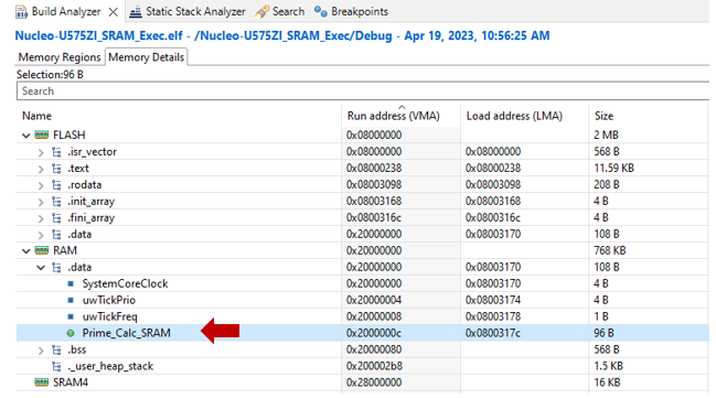
The point here as described in step 12, the linker resolves the function from Flash address 0x0800317C and copies it at startup in SRAM1 at address 0x2000000C.
15. Place two breakpoints:
- In Reset_Handler at line bl SystemInit in startup_stm32u575zitxq.s
- In Prime_Calc_SRAM() function at line primes_ram[0] = 1;
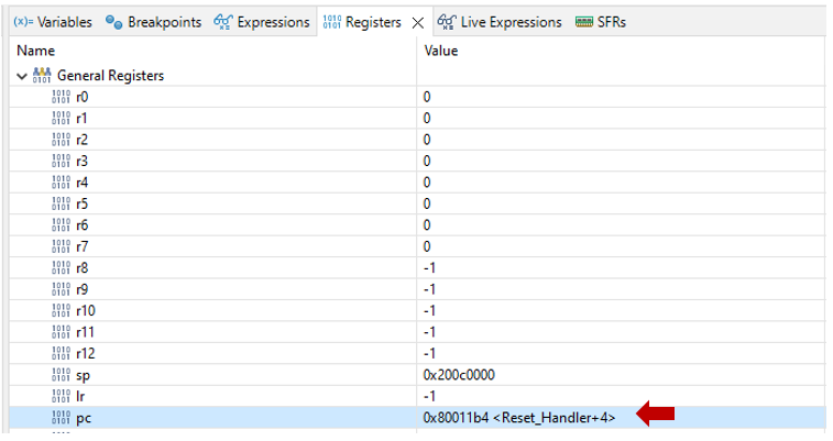
18. We can see that the linker placed the function starting at 0x0800317C and with a size of 96 bytes, in the flash memory section.

19. While the SRAM1 contains random data (or not allocated) at 0x2000000C address.

That means that the code is executed in flash.
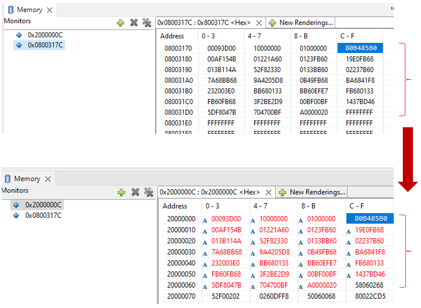
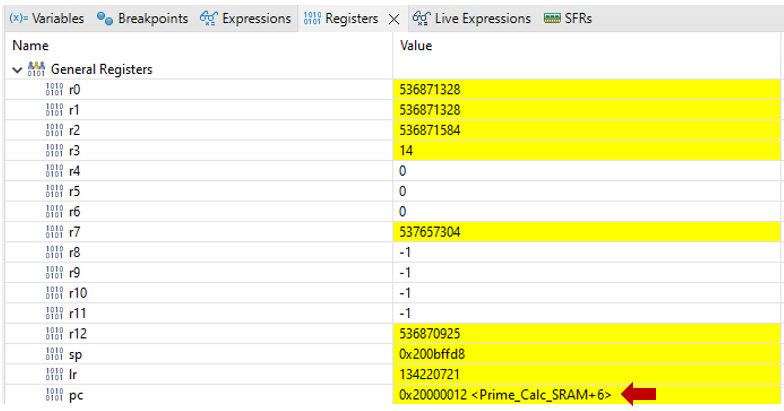
In addition, the 96 bytes of code related to the Prime_Calc_SRAM() function is copied from flash memory at 0x0800317C to SRAM at 0x2000000C.
The copy was done by LoopCopyDataInit: in startup_stm32u575zitxq.s
An other method is to use the existing __RAM_FUNC define (in stm32u5xx_hal_def.h) to declare a function to be executed in SRAM.
#define __RAM_FUNC HAL_StatusTypeDef __attribute__((section(".RamFunc")))Case 2: Placing and executing interrupts in SRAM
This second part describes the steps to link and execute interrupts in SRAM using STM32CubeIDE.It is based on the same project used in the previous steps.
1. Open Nucleo-U575ZI_SRAM_Exec.ioc in order to configure an EXTI interrupts for the User button on the NUCLEO-U575ZI-Q board.
3. Save the project and regenerate the code.
5. Place a Breakpoint in stm32u5xx_it.c at line:
HAL_GPIO_EXTI_IRQHandler(USER_BUTTON_Pin);
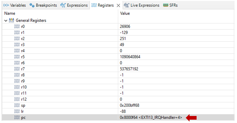
7. Check the Registers → General Registers watch expression, the PC counter is in flash memory.
That is means the interrupt handler function is executed in flash.
8. Stop the debugger.
9. Change the EXTI13_IRQHandler name by applying the same attribute keyword than the previous case.
Add the __attribute__((section(".RamFunc"))) keyword.
/**
  * @brief This function handles EXTI Line13 interrupt.
  */
void __attribute__((section(".RamFunc"))) EXTI13_IRQHandler(void)
{
  /* USER CODE BEGIN EXTI13_IRQn 0 */

  /* USER CODE END EXTI13_IRQn 0 */
  HAL_GPIO_EXTI_IRQHandler(USER_BUTTON_Pin);
  /* USER CODE BEGIN EXTI13_IRQn 1 */

  /* USER CODE END EXTI13_IRQn 1 */
}
12.Check the Registers → General Registers watch expression, the PC counter is at address 0x20000070.
That means that the interrupt handler function is executed in SRAM1.
13. Select Run → Remove all Breakpoints and stop the debug session.
Conclusion: This example is equivalent to the previous chapter. It can be used to place and execute a single or several interrupts’ handlers in the embedded SRAM.
Case 3: Placing and executing an entire project in SRAM (code and interrupts)
This third part describes the steps to link and execute a full STM32 project in SRAM using STM32CubeIDE.
It is still based on the same project used in the previous steps.
Note: For Prime_Calc_SRAM() you must change the prototype and function definition.
2. Open system_stm32u5xx.c and search for #define VECT_TAB_SRAM symbol.
Uncomment the corresponding line (see below)
/************************* Miscellaneous Configuration ************************/
/*!< Uncomment the following line if you need to relocate your vector Table in
Internal SRAM. */
#define VECT_TAB_SRAM
#define VECT_TAB_OFFSET 0x00000000UL /*!< Vector Table base offset field.
This value must be a multiple of 0x200. */
/******************************************************************************/3. Add the following code in the main while(1) loop, it will be useful later:
/* Infinite loop */
/* USER CODE BEGIN WHILE */
while (1)
{
HAL_GPIO_TogglePin(LED_BLUE_GPIO_Port, LED_BLUE_Pin);
HAL_Delay(250);
/* USER CODE END WHILE */4. Check and locate in Project Explorer the linker file generated by CubeMX.
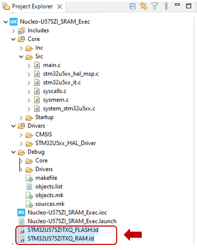
5. As explained in the first case, CubeMX generates two types of linker file.
- STM32U575ZITXQ_FLASH.ld is related to defining all physical memory of the device, like flash memory and all SRAM bank, and to place all the symbols in these sections.
- STM32U575ZITXQ_RAM.ld define only the RAM memory of the device (see below)
/* Memories definition */
MEMORY
{
  RAM	  (xrw)	: ORIGIN = 0x20000000,	LENGTH = 768K
  SRAM4   (xrw)	: ORIGIN = 0x28000000,	LENGTH = 16K
}
Example for the .isr_vector (interrupts) and .text (Code) Sections.
/* The startup code into "RAM" Ram type memory */
  .isr_vector :
  {
    KEEP(*(.isr_vector)) /* Startup code */
  } >RAM

  /* The program code and other data into "RAM" Ram type memory */
  .text :
  {
    *(.text)           /* .text sections (code) */
    *(.text*)          /* .text* sections (code) */
…
…
    KEEP (*(.init))
    KEEP (*(.fini))

    _etext = .;        /* define a global symbols at end of code */
} >RAM7. Go to C/C++ Build → Settings and select the Tool Settings tab.
8. Select MCU GCC Linker → General (see below)
9. Change the Linker Script (-T) path with the following: ${workspace_loc:/${ProjName}/STM32U575ZITXQ_SRAM.ld}
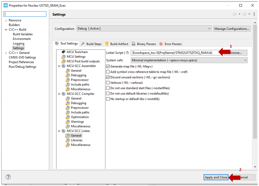
10. Apply and Close to save the new configuration.
11. Clean the project then rebuild it.
12. Check the Build Analyzer that provides an analysis of the new map file generated by the linker configuration.
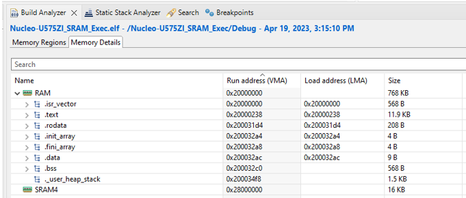
The flash memory section is not present, and all the symbols are placed in SRAM1 (interrupt vector, code, and data.)
13. To be sure that the new project will be executed from SRAM1, we use STM32CubeProgrammer to perform a full chip erase of the flash memory.
14. Open STM32CubeProgrammer, connect to the board and select Full chip erase Icon on the bottom-left corner.
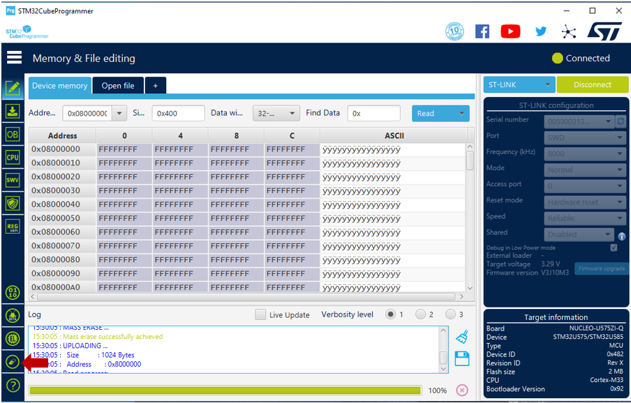
15. The flash memory is erased to 0xFFFFFFFF value.
16. Disconnect the Nucleo board from STM32CubeProgrammer.
17. In STM32CubeIDE, start the debugger and step over to check the same features as the case 1 and 2 as:
- EXTI13_IRQHandler when User button is pressed.
- The result of the Prime_Calc_RAM() function result.
- The blue LED blinking.
If the Nucleo board is powered off, the SRAM loses all the data, and you need to start a new debug session to load and execute the code again.
18. Stop the debugger. Simply press the Reset button on the board (black button) to reboot and restart the firmware: The blue LED2 blinks.
19. The blue LED does not blink, the code is not executed? The board was not powered off, why the code does not restart?
20. Even if we configure all the project to place and execute the full code in SRAM, all the STM32 had a boot mode, which selects what memory address the processor uses to boot at startup.
For the STM32U5 family, you must refer to RM0456, chapter 4 "boot modes".
The same chapter is also present for all other STM32 in their respective Reference Manual.
Table 25 in RM0456 explains the boot mode when TZ=0 (Nonsecure mode)
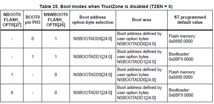
By default, on a new fresh STM32U5, the memory used for boot mode is the flash memory.
It depends on BOOT0 PH3 pin level, in our case, this pin is connected to VSS through a resistor.
We just need to change the NSBOOTADD0[24:0] defined by user option bytes, and configure the boot mode in SRAM1 address, to be aligned with our linker configuration.
21. Open STM32CubeProgrammer, and establish a connection with the board.
22. On the left, select the Option bytes icon.
23. Select Boot Configuration, you should see the NSBOOTADD0 field (see below)
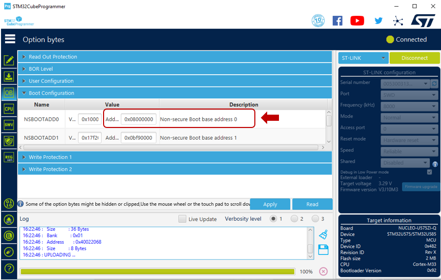
24. Change the value of NSBOOTADD0 Address to 0x20000000. And click Apply to write the new option byte value in the flash memory of the STM32.
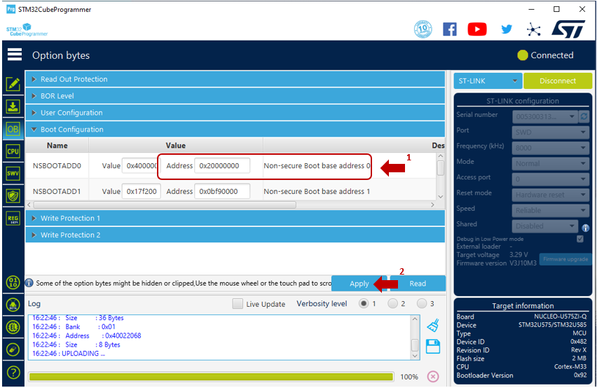
25. Observe the blue LED2, it blinks again. This is because a reset of the STM32U5 has been performed after the write sequence of the NSBOOTADD0. As the board was still powered on during this sequence, the contents of the SRAM1 are not lost, and the firmware can start the execution in SRAM1 again.
Conclusion
This tutorial showed the important steps to place and run a project and its entire code from SRAM1 as an example:- A in application programing firmware.
- A low-power application that powers down the flash memory to reduce the power consumption.
Any other IDE environments such as IAR-EWARM or KEIL-ARM may handle the same project configuration, please refer to their respective documentation to understand the syntax of the linkers.
- Mark as Read
- Mark as New
- Bookmark
- Permalink
- Email to a Friend
- Report Inappropriate Content
This article is fantastic, you should share it more widely on the ST Community forum and make it more visible.
- Mark as Read
- Mark as New
- Bookmark
- Permalink
- Email to a Friend
- Report Inappropriate Content
Hi @etheory (Community Member)
Thank you for your feedback, I'm glad if this article can helps.
For sure, there will be some other publication, it's on the plan.
BR
Romain,
- Mark as Read
- Mark as New
- Bookmark
- Permalink
- Email to a Friend
- Report Inappropriate Content
One quick note on the above.
In my own tests if I use:
static void __attribute__((section(".RamFunc"))) Prime_Calc_SRAM(void)it doesn't work, if I instead use:
void __attribute__((section(".RamFunc"))) Prime_Calc_SRAM(void)then it works.
Is there any reason for this?
Thanks.
- Mark as Read
- Mark as New
- Bookmark
- Permalink
- Email to a Friend
- Report Inappropriate Content
How could I use the above technique to place specific code into CCM RAM? I don't see any logical extension to the above technique.
I note that the .RamFunc definition in the .data section in the linker seems disconnected from the memory RAM definition, so it's unclear how you could successfully add new sections.
- Mark as Read
- Mark as New
- Bookmark
- Permalink
- Email to a Friend
- Report Inappropriate Content
Hi @etheory (Community Member)
Concerning your first note above.
The static C language keyword is defining the limited scope of the declared function, here Prime_Calc_SRAM().
Of course check in your own test that both Prime_Calc_SRAM() prototype and function declaration use the same static keyword.
And your second point:
If you plan to use Core Coupled Memory or multi banks of memory, you must add a new memory section in the linker file.
As an example:
MEMORY
{
...
CCMRAM (rw) : ORIGIN = 0x10000000, LENGTH = 64K
...
}
And now I believe you can change :
} >RAM AT> FLASH
by
} >CCMRAM AT> FLASH
These topic is specific to gnu linker script syntax, and you should find resource on the web.
Using LD, the GNU linker - Command Language
BR
Romain,
- Mark as Read
- Mark as New
- Bookmark
- Permalink
- Email to a Friend
- Report Inappropriate Content
I gave it a go myself but couldn't get it working with a Nucleo-G474RE. What I tried was the following:
For the linker script, STM32G474RETX_FLASH.ld, hange the default:
/* Memories definition */
MEMORY
{
  RAM    (xrw)    : ORIGIN = 0x20000000,   LENGTH = 128K
  FLASH    (rx)    : ORIGIN = 0x8000000,   LENGTH = 512K
}
to:
/* Memories definition */
MEMORY
{
  CCMRAM (xrw)    : ORIGIN = 0x10000000,   LENGTH = 32K
  RAM    (xrw)    : ORIGIN = 0x20000000,   LENGTH = 128K
  FLASH    (rx)    : ORIGIN = 0x8000000,   LENGTH = 512K
}
Then also add:
/* Used by the startup to initialize ccm_data */
  _ccm_sidata = LOADADDR(.ccm_data);

  /* Initialized data sections into "CCMRAM" Ram type memory */
  .ccm_data :
  {
    . = ALIGN(4);
    _ccm_sdata = .;        /* create a global symbol at data start */
    *(.ccm_data)           /* .ccm_data sections */
    *(.ccm_data*)          /* .ccm_data* sections */
    *(.CCMRamFunc)        /* .CCMRamFunc sections */
    *(.CCMRamFunc*)       /* .CCMRamFunc* sections */

    . = ALIGN(4);
    _ccm_edata = .;        /* define a global symbol at data end */

  } >CCMRAM AT> FLASH
Then add to the startup script startup_stm32g474retx.s:
.global	g_pfnVectors
.global	Default_Handler

/* MY MODIFICATION HERE */
.word	_ccm_sidata
.word	_ccm_sdata
.word	_ccm_edata

/* start address for the initialization values of the .data section.
defined in linker script */
.word	_sidata
/* start address for the .data section. defined in linker script */
.word	_sdata
/* end address for the .data section. defined in linker script */
.word	_edata
/* start address for the .bss section. defined in linker script */
.word	_sbss
/* end address for the .bss section. defined in linker script */
.word	_ebss
and:
/* Copy the data segment initializers from flash to SRAM */
  ldr r0, =_sdata
  ldr r1, =_edata
  ldr r2, =_sidata
  movs r3, #0
  b	LoopCopyDataInit

/* MY MODIFICATION HERE */
/* Copy the data segment initializers from flash to CCM SRAM */
  ldr r0, =_ccm_sdata
  ldr r1, =_ccm_edata
  ldr r2, =_ccm_sidata
  movs r3, #0
  b	LoopCopyDataInit
Then to call my function:
void __attribute__((section(".CCMRamFunc"))) run_test(void)I even get the results visible in the STM32CubeIDE Build Analyzer:
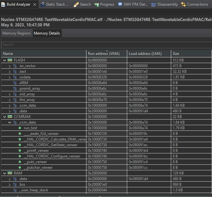
If I switch the code pragma back to:
void __attribute__((section(".RamFunc"))) run_test(void)it's fine.
So I'm confused. What did I miss?
When I run it through the debugger, the second it calls my function run_test, it immediately hits the function:
void HardFault_Handler(void)but I don't know why.
- Mark as Read
- Mark as New
- Bookmark
- Permalink
- Email to a Friend
- Report Inappropriate Content
- Mark as Read
- Mark as New
- Bookmark
- Permalink
- Email to a Friend
- Report Inappropriate Content
I fixed my bug. Everything above is correct except for the .s file, which is now:
/* Copy the data segment initializers from flash to SRAM */
  ldr r0, =_sdata
  ldr r1, =_edata
  ldr r2, =_sidata
  movs r3, #0
  b	LoopCopyDataInit

CopyDataInit:
  ldr r4, [r2, r3]
  str r4, [r0, r3]
  adds r3, r3, #4

LoopCopyDataInit:
  adds r4, r0, r3
  cmp r4, r1
  bcc CopyDataInit

/* MY CHANGES BELOW */
/* Copy the data segment initializers from flash to CCM SRAM */
  ldr r0, =_ccm_sdata
  ldr r1, =_ccm_edata
  ldr r2, =_ccm_sidata
  movs r3, #0
  b	CCMLoopCopyDataInit

CCMCopyDataInit:
  ldr r4, [r2, r3]
  str r4, [r0, r3]
  adds r3, r3, #4

CCMLoopCopyDataInit:
  adds r4, r0, r3
  cmp r4, r1
  bcc CCMCopyDataInit
And now it works.
- Mark as Read
- Mark as New
- Bookmark
- Permalink
- Email to a Friend
- Report Inappropriate Content
@RomainR. your link above isn't that useful, since I want to only put code into CCM RAM, since that's the option recommended for fastest performance, and your article says only how to put data there, which doesn't seem to be a good idea. Only data or code should go there, and for best performance, only code. At least that's what the data sheets say.
If people follow my above post, they can successfully do that, and get a nice speed up as a result. They can then choose for code to go in flash (no pragma) SRAM (RamFunc pragma) or CCM SRAM (CCMRamFunc pragma) which is more flexible.
Thanks.
NOTE: putting code into SRAM as per the article actually made my code run SLOWER due to bus contention. Putting data in SRAM and code in CCM SRAM took my runtime usage statistics from 68.1% to 55.68% which is absolutely incredible.
- Mark as Read
- Mark as New
- Bookmark
- Permalink
- Email to a Friend
- Report Inappropriate Content
Your technique has allowed you to improve the performance of your application, that's a very good point. And thank you for sharing it.
In complement, the AN4296 deals with this topic on STM32F3/G4 devices.
CCM is not available on all products, but I completely agree with you on the interest of being able to place data in SRAM and code in CCM in order to reach the best performance.
Thank you,
BR
Romain,
- Mark as Read
- Mark as New
- Bookmark
- Permalink
- Email to a Friend
- Report Inappropriate Content
Hi @RomainR.
Thanks a lot for your article — it was a huge help!
I can’t go into too much detail about the project (it’s work-related), but we had a use case on an STM32G071 where we needed to:
- Perform a full flash memory erase
- Restore BOOT0 pin functionality
The goal was to allow the chip to boot from system memory so we could reprogram it via the STM bootloader — using any supported method — just like a nearly fresh device.
I say “nearly” because we’ve written some custom IDs into the OTP area.
So that’s another solid reason you might want to add to your list of motivations for running code from RAM in embedded systems.
In our case, the "Case 1" from your article, we also had to explicitly add the noinline and used attributes to make it work, probably for optimization settings I guess:
static void __attribute__((section(".RamFunc"), noinline, used)) XXX_MassEraseAndRestoreBOOT0(void)
Thanks again for sharing your insights — they made a real difference!
Cheers,
Denis
- Mark as Read
- Mark as New
- Bookmark
- Permalink
- Email to a Friend
- Report Inappropriate Content
Hi @DenisBisson
Thank you so much for your message. I’m really glad to hear the article was helpful to you!
It’s always great to see how others apply these techniques in real projects, and your use case sounds like a perfect example. I appreciate you sharing those extra details the note about adding noinline and used keywords is particularly valuable, and I might even update the article to include that insight.
Thanks again for taking the time to write such thoughtful feedback, it truly means a lot!
Best regards,
Romain
- Mark as Read
- Mark as New
- Bookmark
- Permalink
- Email to a Friend
- Report Inappropriate Content
