


How to use XSPI external flash to display an image with LTDC and protect data using MCE
Introduction
The increasing complexity of embedded and graphical applications continues to drive the need for larger memory capacity, faster access performance, and stronger data protection mechanisms.
To address these requirements, STM32 devices integrate high-performance external memory interfaces to connect additional memory resources and protect them. This approach provides an effective solution for storing large graphical assets while ensuring high access and display performance, as well as enhanced data protection through encryption and decryption mechanisms.
1. Project overview
This project illustrates how to configure the MX66UW1G45G external NOR flash memory on the STM32H7S78-DK board using the XSPI2 interface. It also shows how to access an image stored in external flash through memory-mapped mode and display it on the LCD screen via the LTDC controller. In addition, the project uses the MCE peripheral to encrypt and decrypt data stored in external flash memory. If you want to have the edited files at hand immediately, download the extractable file attached at the bottom of the article.
2. Prerequisites
Hardware
Software
- STM32CubeMX version 6.17.0
- STM32CubeIDE version: 2.1.1
3. Steps
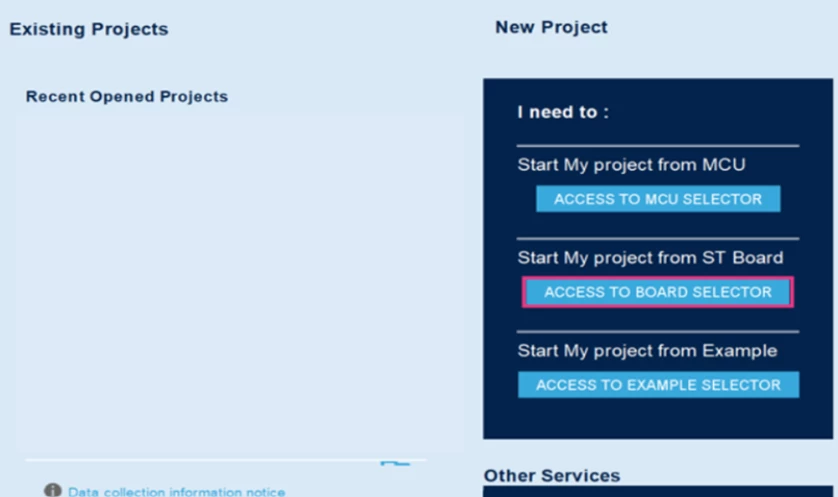
Step 1: Open STM32CubeMX and click the [ACCESS TO BOARD SELECTOR] button.
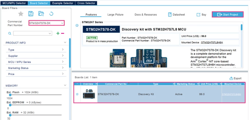
Step 2: Enter the relevant Part Number in the [Commercial Part Number] field. In this example, we use the STM32H7S78-DK board. Select it and click on [Start Project].
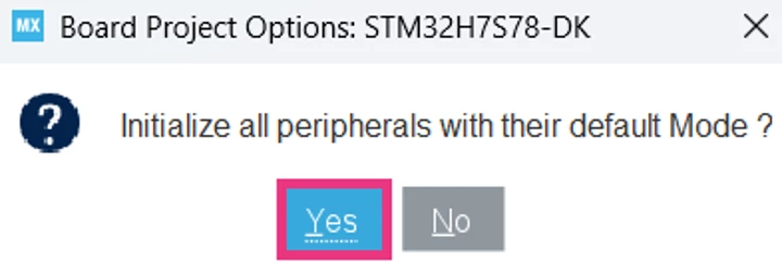
A pop-up appears, as shown in the screenshot below: Click [Yes].
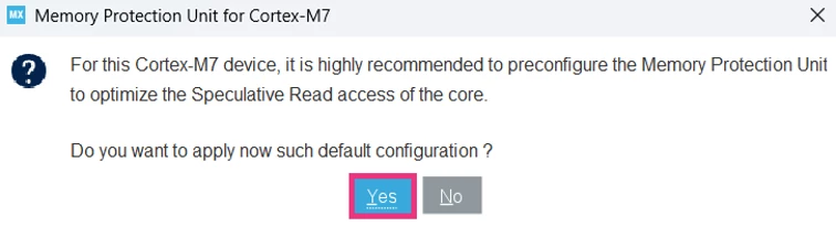
Another pop-up appears, click [Yes].
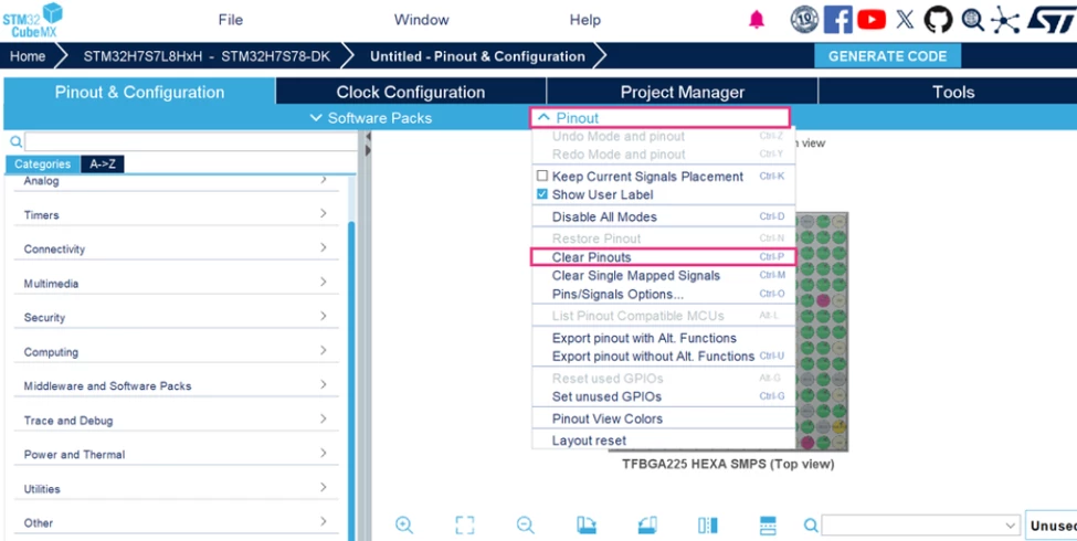
Step 3: Click [Pinout] and then [Clear Pinouts].
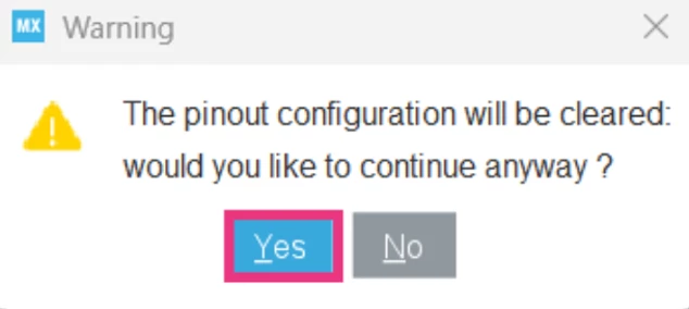
A pop-up appears, as shown in the screenshot below: Click [Yes].
Step 4: XSPI mode and configuration
To access and communicate with the external flash memory, configure the XSPI2 interface as shown in the screenshot below.
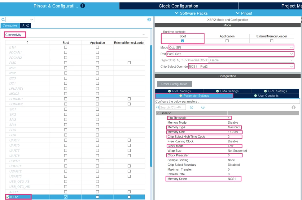
For the GPIO Settings, verify that the XSPI pins are configured in Very High.
Note: For more details about the type of external flash memory and its specifications, as well as the XSPI2 configuration and GPIO settings, refer to this article: “How to configure the external flash memory MX66UW1G45G on the STM32H7S78-DK via XSPI interface".
Step 5: LTDC mode and configuration
To display an image on an LCD-TFT panel driven by the LTDC, several elements must be configured. These elements include the Data format, the Timing parameters, the Display Layers, and the GPIOs. For detailed instructions, refer to this article “How to display an image stored in external flash on the STM32H7S78-DK using the LTDC controller”.
Step 6: MCE mode and configuration
The Memory Cipher Engine (MCE) is a hardware security accelerator integrated into the STM32H7S78 microcontroller. It provides transparent encryption and decryption of data stored in external memories, such as NOR Flash or PSRAM, without processor intervention. In this example, we enable it to encrypt and decrypt the data stored in the external NOR flash memory, as shown in the screenshot below.
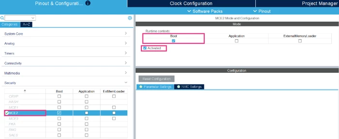
Note: To understand the concept of MCE and get more information on it, refer to this application note: “How to use MCE for encryption/decryption on STM32 MCUs” and consult RM0477 specifically section 39 Memory cipher engine (MCE).
Step 7: SBS mode and configuration
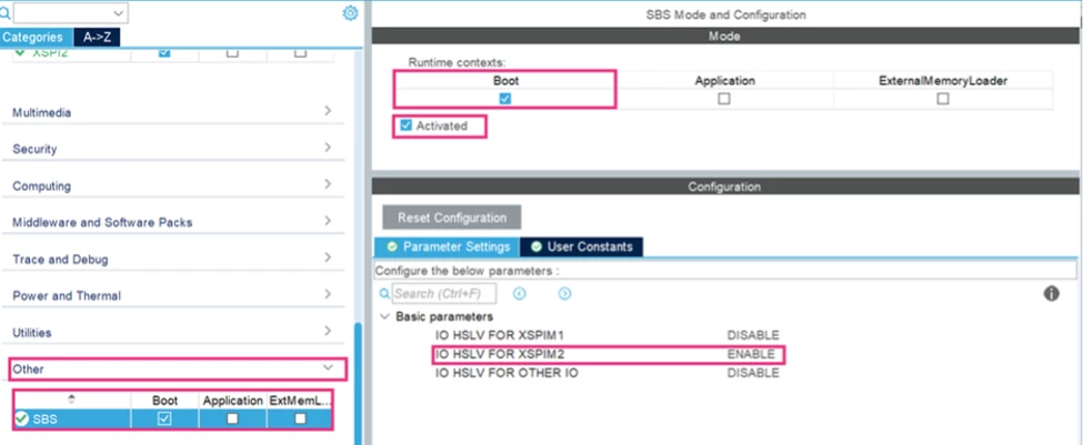
Enabling HSLV is recommended in cases when the XSPIM domain is powered by 1.8 V and operates the serial memory interface at its maximum speed of 200 MHz.
Note: For more details about HSLV, refer to this FAQ: “Recommendations for high-speed low-voltage mode (HSLV) on the STM32H7RS”.
Step 8: Clock configuration
- MCU Clock Frequency = 600 MHz
- f_Kernel = 200 MHz
- LTDC Frequency = 25 MHz
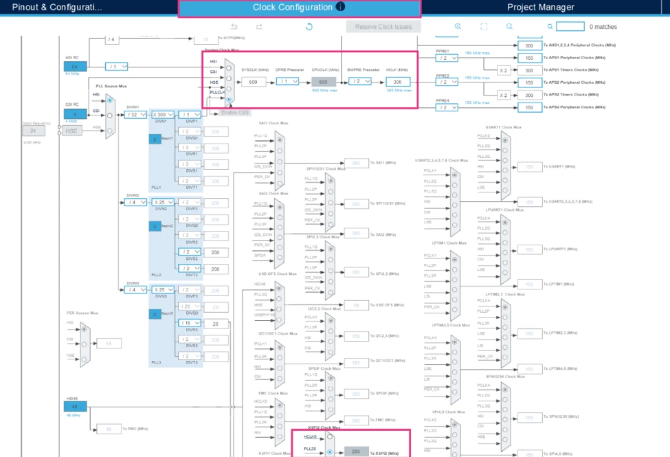
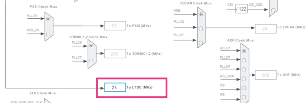
Note: For more details about the LTDC frequency, refer to the KB article: "How to display an image stored in external flash on the STM32H7S78-DK using the LTDC controller".
For the memory management:
Make sure that the configuration is set up as shown in the screenshot below.
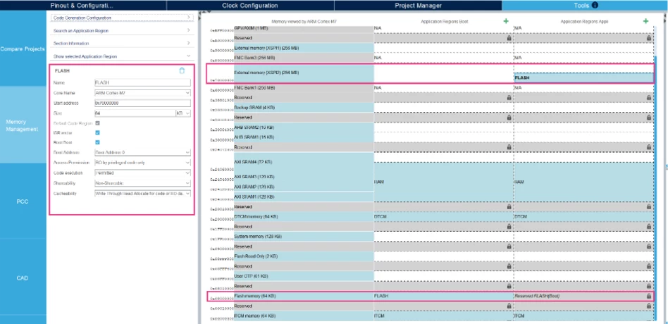
Step 9: Generate code
Enter the Project Name, choose the Toolchain/IDE, and click [GENERATE CODE], as shown in the screenshot below.
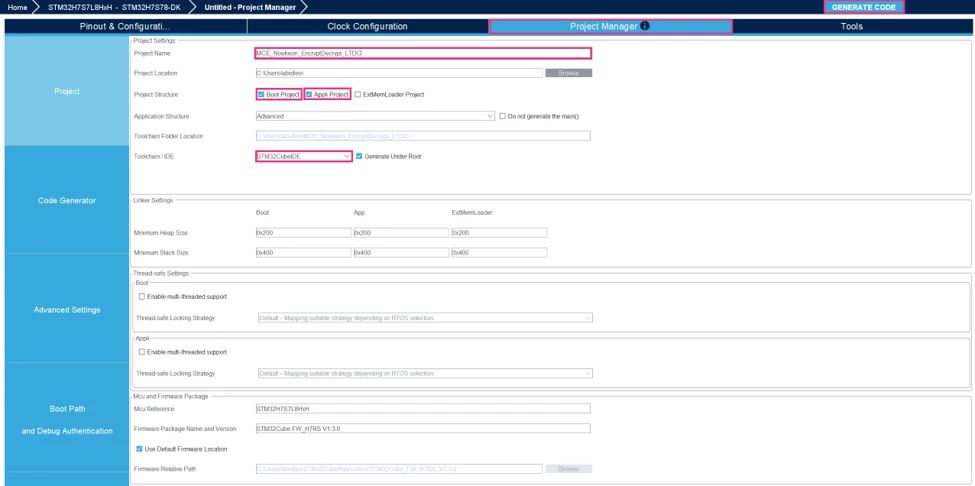
Step 10: Image conversion
To display the image from external flash memory, the picture must be converted into a pixel format compatible with the LTDC framebuffer. This conversion allows the LTDC to read the image directly and show it on the LCD-TFT panel.
To convert the image and generate the header file (Image.h), use the LCD-Image-Converter-20190317 tool by following the steps described in this article: “How to display an image stored in external flash on the STM32H7S78-DK using the LTDC controller”
Step 11: Edit main.c in the Boot project
In main.c, several code sections must be added to configure the MCE2 peripheral and the external flash memory MX66UW1G45G connected via XSPI2. In this project, MCE2 is configured in Noekeon Block Cipher mode.
- Insert private variables declarations
/* MCE configuration structures */
MCE_RegionConfigTypeDef RegionConfig;
MCE_RegionConfigTypeDef RegionConfig_npriv;
MCE_NoekeonConfigTypeDef NoekeonConfig;
MCE_RegionConfigTypeDef config;


/* USER CODE BEGIN PV */
/* cryptographic key used by the MCE Noekeon engine */
uint32_t Key[4][4]     = { { 0x71234567, 0x89ABCDEF, 0x71234567, 0x89ABCDEF },
                           { 0xEDCBA987, 0x6543210F, 0xEDCBA987, 0x6543210F },
                           { 0x23456789, 0xABCDEF01, 0x23456789, 0xABCDEF01 },
                           { 0xCBA98765, 0x43210FED, 0xCBA98765, 0x43210FED }
};
/* USER CODE END PV */- Insert the private functions prototypes
/* USER CODE BEGIN PFP */
/* declare a function used to configure the external flash in Octal DTR mode*/
static void XSPI_NOR_OctalDTRModeCfg(XSPI_HandleTypeDef *hxspi);
/* declare a function used to jump to the application, where we execute our image stored in the external NOR flash memory */
static void JumpToApplication(void);
/* USER CODE END PFP */- In the USER CODE BEGIN 2, insert the following code:
/* USER CODE BEGIN 2 */
  XSPI_NOR_OctalDTRModeCfg(&hxspi2);
         JumpToApplication();
/* USER CODE END 2 */- In the USER CODE BEGIN 4, insert the following code:
/* USER CODE BEGIN 4 */
void HAL_XSPI_ErrorCallback(XSPI_HandleTypeDef *hxspi)
{
Error_Handler();
}
/* this function configures the external NOR flash memory in Octal DTR mode, allowing it to operate with the XSPI interface at high-speed */
static void XSPI_NOR_OctalDTRModeCfg(XSPI_HandleTypeDef *hxspi)
{
XSPI_RegularCmdTypeDef sCommand = {0};
XSPI_AutoPollingTypeDef sConfig = {0};
uint8_t reg = 0x02;
/* enable write operations on the flash memory before modifying any configuration register */
sCommand.OperationType = HAL_XSPI_OPTYPE_COMMON_CFG;
sCommand.Instruction = WRITE_ENABLE_CMD;
sCommand.InstructionMode = HAL_XSPI_INSTRUCTION_1_LINE;
sCommand.InstructionWidth = HAL_XSPI_INSTRUCTION_8_BITS;
sCommand.InstructionDTRMode = HAL_XSPI_INSTRUCTION_DTR_DISABLE;
sCommand.AddressMode = HAL_XSPI_ADDRESS_NONE;
sCommand.AlternateBytesMode = HAL_XSPI_ALT_BYTES_NONE;
sCommand.DataMode = HAL_XSPI_DATA_NONE;
sCommand.DummyCycles = 0;
sCommand.DQSMode = HAL_XSPI_DQS_DISABLE;
if (HAL_XSPI_Command(hxspi, &sCommand, HAL_XSPI_TIMEOUT_DEFAULT_VALUE) != HAL_OK)
{
Error_Handler();
}
/* prepare a status register read command to check when the Write Enable Latch bit becomes active */
sCommand.Instruction = READ_STATUS_REG_CMD;
sCommand.DataMode = HAL_XSPI_DATA_1_LINE;
sCommand.DataLength = 1;
/* Configure automatic polling to wait until the WEL bit is set */
sConfig.MatchMode = HAL_XSPI_MATCH_MODE_AND;
sConfig.MatchValue = WRITE_ENABLE_MATCH_VALUE;
sConfig.MatchMask = WRITE_ENABLE_MASK_VALUE;
sConfig.AutomaticStop = HAL_XSPI_AUTOMATIC_STOP_ENABLE;
sConfig.IntervalTime = 0x10;
/*send the status register read command*/
if (HAL_XSPI_Command(hxspi, &sCommand, HAL_XSPI_TIMEOUT_DEFAULT_VALUE) != HAL_OK)
{
Error_Handler();
}
/* poll the flash status until write enable is confirmed */
if (HAL_XSPI_AutoPolling(hxspi, &sConfig, HAL_XSPI_TIMEOUT_DEFAULT_VALUE) != HAL_OK)
{
Error_Handler();
}
/* write the configuration register to switch the flash to the Octal I/O protocol */
sCommand.Instruction = WRITE_CFG_REG_2_CMD;
sCommand.AddressMode = HAL_XSPI_ADDRESS_1_LINE;
sCommand.AddressWidth = HAL_XSPI_ADDRESS_32_BITS;
sCommand.Address = 0;
sCommand.DataMode = HAL_XSPI_DATA_1_LINE;
sCommand.DataLength = 1;
/* send the configuration register write command */
if (HAL_XSPI_Command(hxspi, &sCommand, HAL_XSPI_TIMEOUT_DEFAULT_VALUE) != HAL_OK)
{
Error_Handler();
}
/* write the value that enables Octal mode */
if (HAL_XSPI_Transmit(hxspi, ®, HAL_XSPI_TIMEOUT_DEFAULT_VALUE) != HAL_OK)
{
Error_Handler();
}
}
/* this function prepares the flash for memory-mapped access, configures the MCE protection region, and then jumps to the application stored in external flash memory */
typedef void (*pFunction)(void);
static void JumpToApplication(void)
{
/* function pointer used to jump to the application's reset handler */
pFunction JumpToApp;
/* base address of the application vector table in external NOR flash */
uint32_t Application_vector = 0x70000000U;
/* XSPI command structure used to configure read and write accesses */
XSPI_RegularCmdTypeDef sCommand = {0};
/* memory-mapped configuration structure for XSPI */
XSPI_MemoryMappedTypeDef sMemMappedCfg= {0};
/* Configure the write sequence for the external flash in Octal DTR mode */
sCommand.OperationType = HAL_XSPI_OPTYPE_WRITE_CFG;
sCommand.IOSelect = HAL_XSPI_SELECT_IO_7_0;
sCommand.Instruction = OCTAL_PAGE_PROG_CMD;
sCommand.InstructionMode = HAL_XSPI_INSTRUCTION_8_LINES;
sCommand.InstructionWidth = HAL_XSPI_INSTRUCTION_16_BITS;
sCommand.InstructionDTRMode = HAL_XSPI_INSTRUCTION_DTR_ENABLE;
sCommand.Address = 0;
sCommand.AddressMode = HAL_XSPI_ADDRESS_8_LINES;
sCommand.AddressWidth = HAL_XSPI_ADDRESS_32_BITS;
sCommand.AddressDTRMode = HAL_XSPI_ADDRESS_DTR_ENABLE;
sCommand.AlternateBytes = 0;
sCommand.AlternateBytesMode = HAL_XSPI_ALT_BYTES_NONE;
sCommand.AlternateBytesWidth = 0;
sCommand.AlternateBytesDTRMode = 0;
sCommand.DataMode = HAL_XSPI_DATA_8_LINES;
sCommand.DataLength = 1;
sCommand.DataDTRMode = HAL_XSPI_DATA_DTR_ENABLE;
sCommand.DummyCycles = 0;
sCommand.DQSMode = HAL_XSPI_DQS_DISABLE;
/* send the write configuration command to set the flash access mode */
if (HAL_XSPI_Command(&hxspi2, &sCommand, HAL_XSPI_TIMEOUT_DEFAULT_VALUE)!= HAL_OK)
{
Error_Handler();
}
/* reconfigure XSPI for read access in Octal DTR mode */
sCommand.OperationType = HAL_XSPI_OPTYPE_READ_CFG;
sCommand.Instruction = OCTAL_IO_DTR_READ_CMD;
sCommand.DummyCycles = DUMMY_CLOCK_CYCLES;
sCommand.DQSMode = HAL_XSPI_DQS_ENABLE;
/* read configuration */
if (HAL_XSPI_Command(&hxspi2, &sCommand, HAL_XSPI_TIMEOUT_DEFAULT_VALUE) != HAL_OK)
{
Error_Handler();
}
/* enable memory-mapped mode so that the external flash memory can be accessed directly using a memory address */
sMemMappedCfg.TimeOutActivation = HAL_XSPI_TIMEOUT_COUNTER_DISABLE;
sMemMappedCfg.TimeoutPeriodClock = 0;
if (HAL_XSPI_MemoryMapped(&hxspi2, &sMemMappedCfg) != HAL_OK)
{
Error_Handler();
}
/* configure the MCE to protect the data stored in external flash. */
NoekeonConfig.KeyType = MCE_USE_MASTERKEYS;
NoekeonConfig.pKey = Key[2];
if (HAL_MCE_ConfigNoekeon(&hmce2, &NoekeonConfig) != HAL_OK)
{
Error_Handler();
}
/* define the flash memory region to be protected by the MCE*/
RegionConfig.Mode = MCE_BLOCK_CIPHER;
RegionConfig.ContextID = MCE_NO_CONTEXT;
RegionConfig.StartAddress = 0x70000000;
RegionConfig.EndAddress = 0x7FFFFFFF;
RegionConfig.PrivilegedAccess = MCE_REGION_NPRIV;
RegionConfig.AccessMode = MCE_REGION_READWRITE;
/* Apply the MCE region configuration */
if (HAL_MCE_ConfigRegion(&hmce2, 0, &RegionConfig) != HAL_OK)
{
Error_Handler();
}
/* disable configuration of MCE region*/
if (HAL_MCE_DisableRegion(&hmce2, 0) != HAL_OK)
{
Error_Handler();
}
/* read the reset handler address of the application from the vector table */
JumpToApp = (pFunction)(*(__IO uint32_t *)(Application_vector + 4U));
/* jump to the application */
JumpToApp();
}
/* USER CODE END 4 */Step 12: Edit main.h in the Boot project
- The private definition can be added to main.h
/* USER CODE BEGIN EC */
/* MX66UW1G45G macronix memory */
/* Flash commands */
#define OCTAL_IO_DTR_READ_CMD 0xEE11
#define OCTAL_PAGE_PROG_CMD 0x12ED
#define READ_STATUS_REG_CMD 0x05
#define WRITE_CFG_REG_2_CMD 0x72
#define WRITE_ENABLE_CMD 0x06
/* dummy clocks cycles */
#define DUMMY_CLOCK_CYCLES 20
/* auto-polling values */
#define WRITE_ENABLE_MATCH_VALUE 0x02
#define WRITE_ENABLE_MASK_VALUE 0x02
/* USER CODE END EC */
Note: When the MCE is used together with XSPI, it is mandatory to access the flash memory through the memory-mapped mode of the flash memory controller.
Step 13: Edit main.c in the application project
In main.c, we need to add the generated header file (Image.h) and the framebuffer start address used by the LTDC.
- Insert Image.h in Private includes section
/* USER CODE BEGIN Includes */
#include "Image.h"
/* USER CODE END Includes */- Set the framebuffer start address used by the LTDC:
pLayerCfg.WindowX0 = 0;
  pLayerCfg.WindowX1 = 800;
  pLayerCfg.WindowY0 = 0;
  pLayerCfg.WindowY1 = 480;
  pLayerCfg.PixelFormat = LTDC_PIXEL_FORMAT_RGB565;
  pLayerCfg.Alpha = 255;
  pLayerCfg.Alpha0 = 0;
  pLayerCfg.BlendingFactor1 = LTDC_BLENDING_FACTOR1_PAxCA;
  pLayerCfg.BlendingFactor2 = LTDC_BLENDING_FACTOR2_PAxCA;
  pLayerCfg.FBStartAdress = (uint32_t)image_data_Image;
  pLayerCfg.ImageWidth = 800;
  pLayerCfg.ImageHeight = 480;
  pLayerCfg.Backcolor.Blue = 0;
  pLayerCfg.Backcolor.Green = 0;
  pLayerCfg.Backcolor.Red = 0;
Note:
- The frame buffer start address value is found in the Image.h file, as shown in the screenshot below.
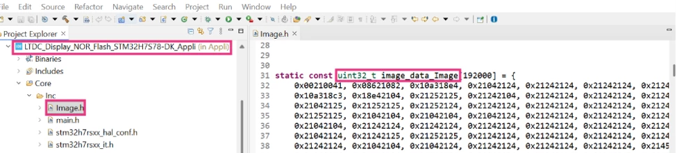
In the same file (Image.h), the user must comment out the structure definition. This definition is located just after the table and keep only the table definition, as shown in the screenshot below.

Step 14: Build the application project
- Click the [Build] button.
Step 15: Debug and verification
To debug the project without flashing the boot every time, follow the steps described in this article: “STM32CubeIDE: How to debug an STM32H7Rx/Sx project without flashing boot every time”.
Click the [Resume] button.
The screenshot below shows the image on the LCD panel. This confirms that the framebuffer content is stored correctly in external flash memory and rendered by the LTDC. Meanwhile, MCE2 handles the encryption and decryption of data.
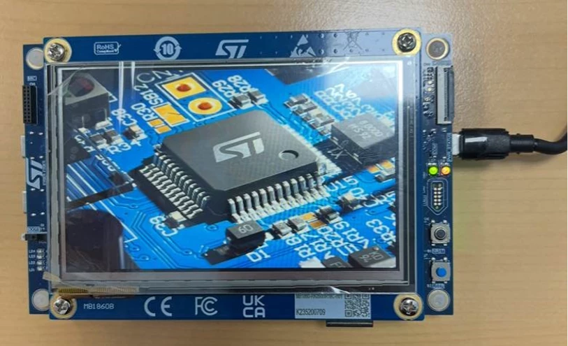
For further verification:
- Click on [Window], then select [Memory Browser]. Enter the corresponding address of the memory-mapped external flash, accessed through XSPI2. The address is “0x70000000”, as shown in the screenshot below.
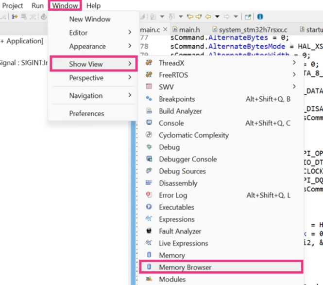

Note: The XSPI2 Base Address “0x70000000” can be found in the reference manual RM0477.
Set breakpoints on the following instructions to pause execution at key stages of the Boot sequence. It helps control access to external flash memory and validates the MCE configuration.
- if (HAL_XSPI_MemoryMapped(&hxspi2, &sMemMappedCfg) != HAL_OK),
click [Resume]. Then use [Step Over] to verify that the external flash memory is correctly accessible in memory-mapped mode and its content.
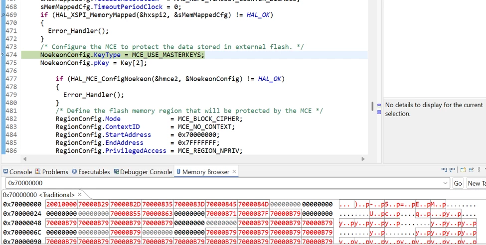
The raw data stored in external memory becomes directly accessible and visible at this address once the application enters memory-mapped mode.
- if (HAL_MCE_ConfigRegion(&hmce2, 0, &RegionConfig) != HAL_OK), click [Resume]. Then use [Step Over] to verify the encrypted region managed by the MCE peripheral, as shown in the screenshot below.
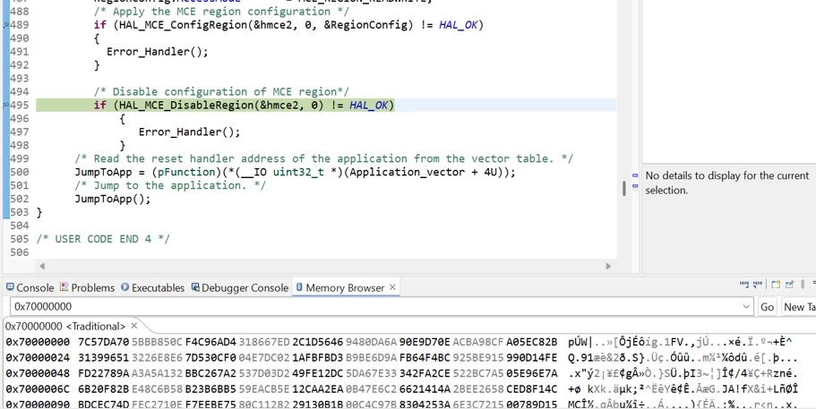
Once the MCE region is configured, the external flash content is no longer handled as plain text. This confirms that the protection mechanism is correctly applied.
• if (HAL_MCE_DisableRegion(&hmce2, 0) != HAL_OK), click [Resume]. Then use [Step Over] to verify that the protected region returns to clear data when the HAL_MCE_DisableRegion() function is executed.
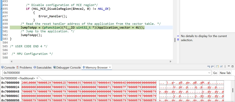
When the system disables the MCE region, the protected memory content becomes clear data. This shows that the encryption mechanism is no longer applied.
Conclusion
After following this guide, the user can configure the MX66UW1G45G external flash memory on the STM32H7S78-DK using XSPI2. They can display an image stored in the external flash on the LCD using LTDC. They can also protect data in the dedicated memory region by using the MCE peripheral.
Related links
- Knowledge article: How to configure the external flash memory MX66UW1G45G on the STM32H7S78-DK via XSPI interface
- Knowledge article: How to display an image stored in external flash on the STM32H7S78-DK using the LTDC controller
- Application note AN6088: How to use MCE for encryption/decryption on STM32 MCUs
- FAQ: Recommendations for high-speed low-voltage mode (HSLV) on the STM32H7RS
- STM32CubeIDE: How to debug an STM32H7Rx/Sx project without flashing boot every time | Community