


How to configure the external flash memory MX66UW1G45G on the STM32H7S78-DK via XSPI interface
Introduction
Embedded applications are evolving toward increasingly demanding memory requirements. This evolution is due to the growing demand for richer graphics, a wider range of multimedia and other data-intensive content.
To address this need, STM32 devices integrate high-speed external memory interfaces that make it possible to add complementary memory suited to memory-intensive applications.
This article presents a practical example of configuring the external flash memory MX66UW1G45G on the STM32H7S78-DK via XSPI2.
1. Project overview
This project illustrates how to configure the MX66UW1G45G octo-SPI NOR flash memory on the STM32H7S78-DK using the XSPI2 interface.
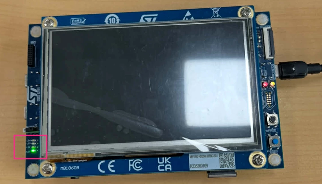
The example configures the memory in Octal DTR mode, performs a sector erase and a page program operation by writing a string into the NOR flash using indirect mode. Finally, it then switches the XSPI peripheral to memory-mapped mode for readback verification. The received data is compared against the transmitted buffer to validate data integrity: a successful match turns on the green LED, while any mismatch activates the red LED.
2. Prerequisites
Hardware
Software
- STM32CubeMX version 6.17.0 or newer
- STM32CubeIDE version: 2.1.1 or newer
3. Steps
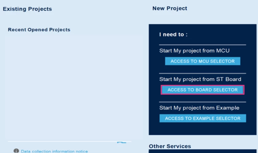
Step 1: Open STM32CubeMX and click the [ACCESS TO BOARD SELECTOR] button.
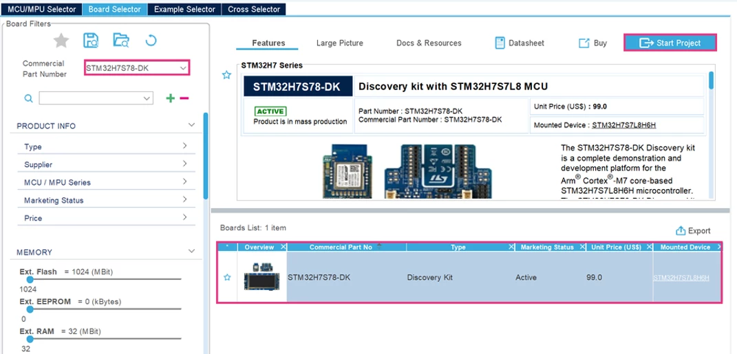
Step 2: Enter the relevant Part Number in the [Commercial Part Number] field. In this example, we use the STM32H7S78-DK. Select it and click on [Start Project].
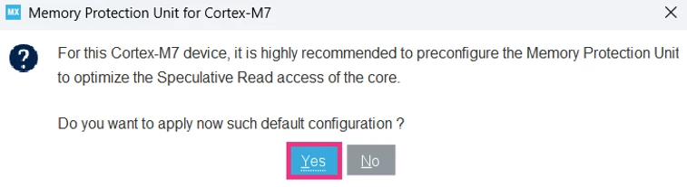
A window opens, as shown in the screenshot below: click [Yes].
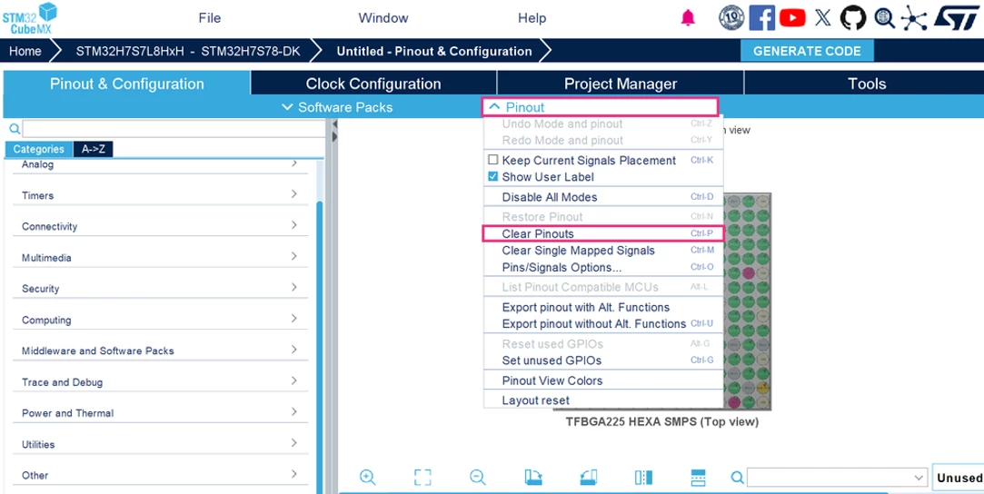
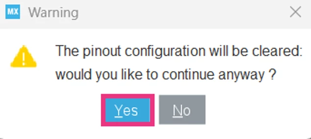
Step 3: Click [Pinout] and then [Clear Pinouts].
A pop-up appears, as shown in the screenshot below: click [Yes].
Step 4: XSPI Mode and configuration
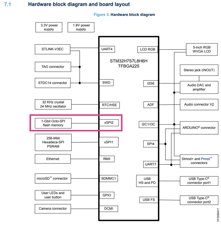
To identify which XSPI interface is used to connect and communicate with the external flash memory on the STM32H7S78-DK board, refer to the user manual UM3289, as shown in the screenshot below.
To identify the memory type on the STM32H7S78-DK, refer to the schematic MB1736 of the board, as shown in the screenshot below.
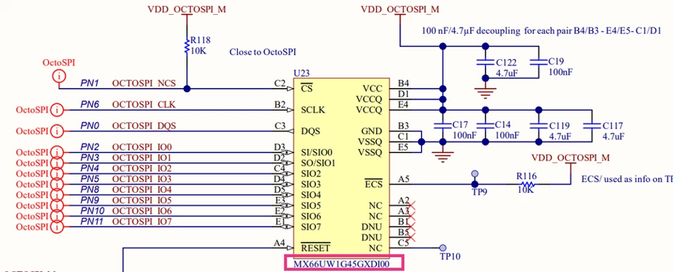
The XSPI interface used is XSPI2, and the memory type is MX66UW1G45GXDI00. Therefore, follow the configuration associated with this interface, as shown in the screenshot below.
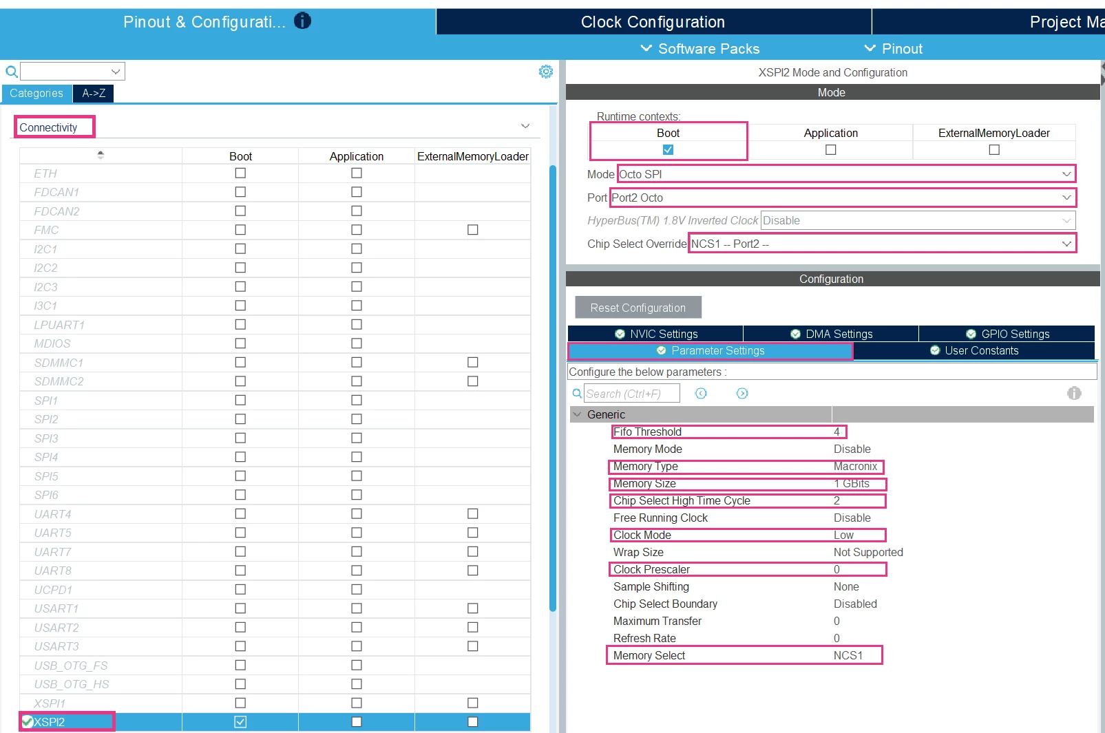
• Runtime contexts = Boot
• Mode = Octo SPI → The external flash memory MX66UW1G45G supports the Octaflash interface.
• Fifo Threshold = 4 → Defines the number of bytes in the FIFO required to trigger certain transfer operations. A value of 4 bytes provides a good compromise between processing speed and transfer efficiency.
• Memory Mode = Disable → Identifies that a single memory is used, it is enabled when using dual memory.
• Memory Type = Macronix → Means that the OCTOSPI interface is configured according to the Macronix protocol used by the external flash memory MX66UW1G45G. It uses a specific bit ordering (D1/D0) on the Serial Input/Output (SIO) lines required.
• Memory Size = 1 GBits → The memory size of MX66UW1G45G is 1 GBits.
• Chip Select High Time (tCSH) = 2 → Defines the chip-select minimum high time in number of clock cycles, configured depending on the memory datasheet, (refer to the MX66UW1G45G Memory Datasheet, specifically in AC CHARACTERISTICS table)
• Free Running Clock = Disable → The clock is not kept running continuously, which reduces power consumption.
• Clock Mode = Low → The clock must stay low while chip select is high (refer to the reference manual RM0477, specifically the NCS behavior section).
• Wrap Size = Not Supported → The automatic wrap-around read mode is not used, because this feature is not needed in our example.
• Clock Prescaler = 0 → The prescaler is used to divide the source clock of the XSPI peripheral (f_) to obtain a frequency compatible with the external flash.
The formula is: f_CLK = f_Kernel/Prescaler+1
Where:
- f_CLK = frequency applied to the memory on the XSPI lines
- f_ Kernel= clock frequency provided to the XSPI peripheral by the MCU
To choose the correct prescaler value, we must verify that the XSPI frequency is supported by both the MCU and the memory.
For f_Kernel = 200 MHz & f_CLK = 200 MHz → therefore, the prescaler value is 0.
• Sample Shifting = 0 → Sample shifting (SSHT) is recommended as enabled in STR mode and disabled in DTR mode.
• Chip Select Boundary = Disabled → Configured depending on the memory datasheet. The chip select must go high when crossing the page boundary (2^CSBOUND bytes defines the page size).
• Maximum transfer = 0 → No specific maximum transfer size is imposed.
• Refresh rate = 0 → Required for PSRAMs memories, NOR flash does not require periodic refresh.
• Memory Select = NCS1 → Selects the CS#1 line for the external memory, because the external flash memory MX66UW1G45G is connected to this line on the STM32H7S78-DK board.
Note: For more details about the configuration of these parameters as shown in the screenshot above, users can refer to the application note AN5050. Specifically, the "STM32CubeMX - Configuration of OCTOSPI parameters" section and the "MX66UW1G45G Memory Datasheet".
For the GPIO settings:
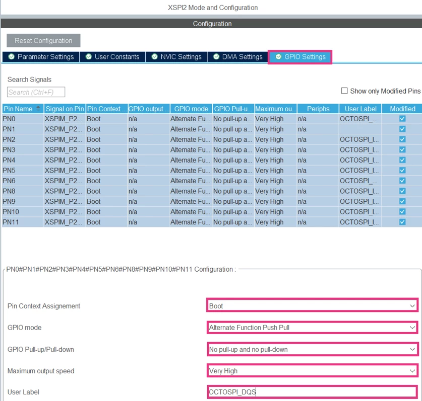
Verify that the pins are configured in this way, as shown in the screenshot above. Verify that the Pin Name is compatible with the Signal on Pin through the schematic of the board MB1736, as shown in the screenshot below.
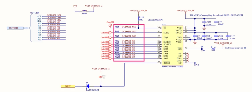
Step 5: GPIO Mode and Configuration
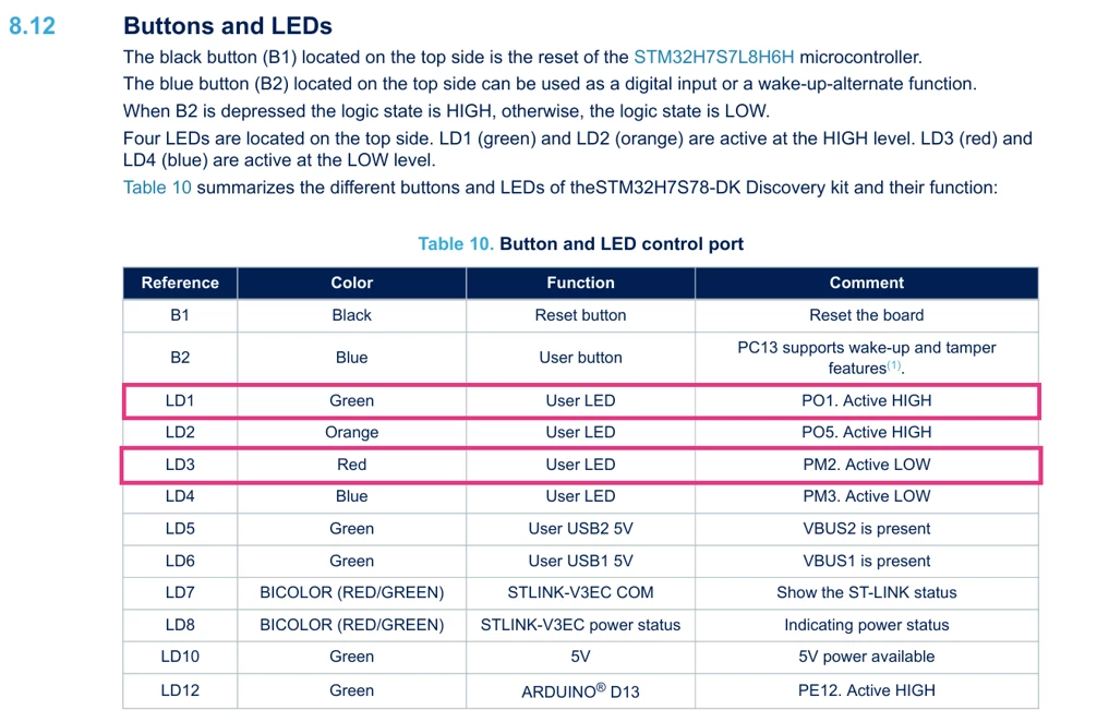
Configure PO1 and PM2 user LED pins (used to check data transfer errors) according to user manual UM3289, as shown in the screenshots below.
Configure them as GPIO Output pins with the following settings, as shown in the screenshot below.
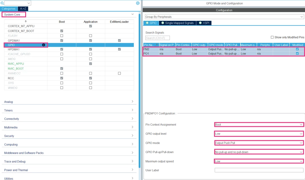
These two GPIO pins are used as visual indicators. The green LED is turned on when the data matches, and the red LED is turned on when an error is detected.
Step 6: SBS Mode and configuration
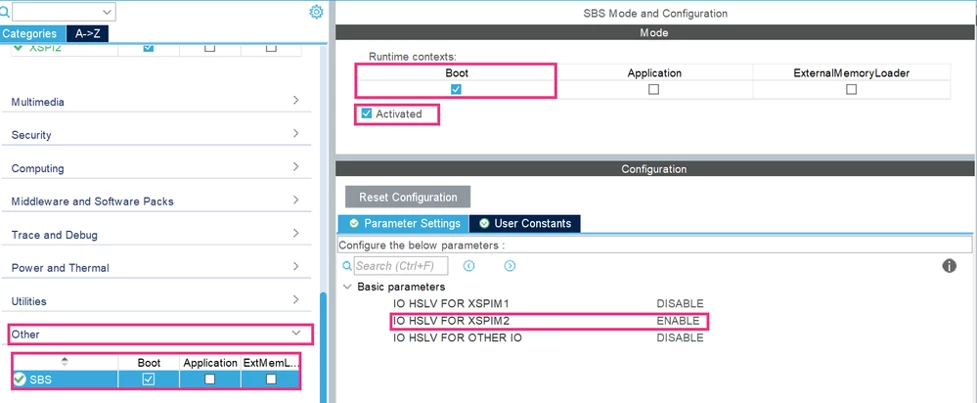
Enabling HSLV is recommended in cases when the XSPIM domain is powered by 1.8 V and is operating the serial memory interface at its maximum speed of 200 MHz.
Note: For more details about HSLV, refer to the Recommendations for high-speed low-voltage mode (HSLV) on the STM32H7RS FAQ.
Step 7: Clock configuration
- MCU clock frequency = 600 MHz
- f_Kernel = 200 MHz
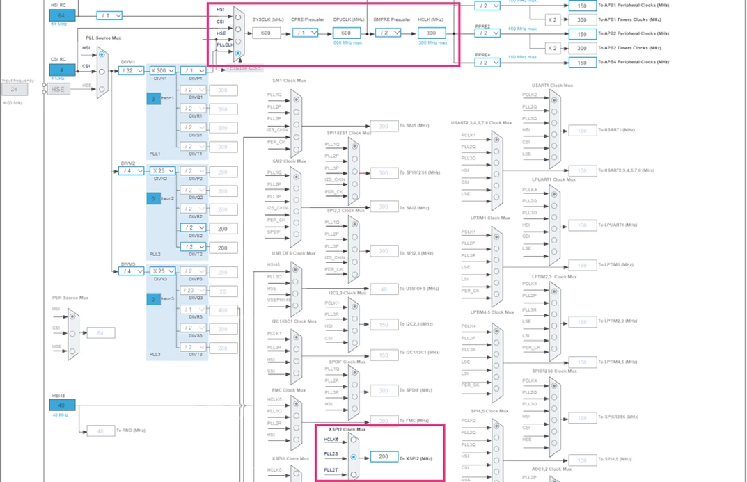
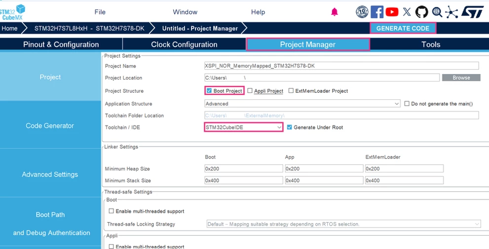
Step 8: Generate Code
Enter the Project Name, choose the Toolchain/IDE and click [GENERATE CODE], as shown in the screenshot below.
Step 9: Edit main.c
After generating the project with STM32CubeMX, several code sections must be added in main.c to configure the external flash memory MX66UW1G45G through XSPI2. Additionally, to run the erase, program, and readback sequence.
- Insert the private variables declarations
/* USER CODE BEGIN PV */
/*variable used to store the XSPI kernel clock frequency*/
uint32_t xspi_ker_freq;
/* Buffer used for transmission */
uint8_t aTxBuffer[] = " Programming in indirect mode - Reading in memory mapped mode ";
__IO uint8_t *nor_memaddr = (__IO uint8_t *)(XSPI2_BASE);
/* Buffer used for reception */
__IO uint8_t aRxBuffer[BUFFERSIZE];
/* USER CODE END PV */
- Insert the private functions prototypes
/* USER CODE BEGIN PFP */
/*Enable write access to the flash (Wait until WEL=1) */
static void XSPI_WriteEnable(XSPI_HandleTypeDef *hxspi);
/*Wait until the flash is ready after an erase or program operation (Wait until WIP=0)*/
static void XSPI_AutoPollingMemReady(XSPI_HandleTypeDef *hxspi);
/*Configure the external flash memory MX66UW1G45G in Octal DTR mode*/
static void XSPI_NOR_OctalDTRModeCfg(XSPI_HandleTypeDef *hxspi);
- In the USER CODE BEGIN 1, insert the following code:
/* USER CODE BEGIN 1 */
       /*Declaration of the XSPI command structure, initialized to zero*/
  XSPI_RegularCmdTypeDef sCommand = {0};
       /*Declaration of the memory-mapped configuration structure, initialized to zero*/
  XSPI_MemoryMappedTypeDef sMemMappedCfg = {0};
/*Local variables used for buffer iteration and error counting*/
  uint16_t index, errorBuffer = 0;
/* USER CODE END 1 */
- In the USER CODE BEGIN 2, insert the following code:
  /* USER CODE BEGIN 2 */
  /* Read the XSPI2 kernel clock frequency for debug and verification */
  xspi_ker_freq = HAL_RCCEx_GetPeriphCLKFreq(RCC_PERIPHCLK_XSPI2);
  /* Initialize Reception buffer ----------------------------- */
  for (index = 0; index < BUFFERSIZE; index++)
  {
    aRxBuffer[index] = 0;
  }
  /* Configure the memory in octal DTR mode ----------------------------------- */
  XSPI_NOR_OctalDTRModeCfg(&hxspi2);
  /* Erasing Sequence --------------------------------------------------------- */
  XSPI_WriteEnable(&hxspi2);
  sCommand.OperationType      = HAL_XSPI_OPTYPE_COMMON_CFG;
  sCommand.Instruction        = OCTAL_SECTOR_ERASE_CMD;
  sCommand.InstructionMode    = HAL_XSPI_INSTRUCTION_8_LINES;
  sCommand.InstructionWidth   = HAL_XSPI_INSTRUCTION_16_BITS;
  sCommand.InstructionDTRMode = HAL_XSPI_INSTRUCTION_DTR_ENABLE;
  sCommand.AddressMode        = HAL_XSPI_ADDRESS_8_LINES;
  sCommand.AddressWidth       = HAL_XSPI_ADDRESS_32_BITS;
  sCommand.AddressDTRMode     = HAL_XSPI_ADDRESS_DTR_ENABLE;
  sCommand.AlternateBytesMode = HAL_XSPI_ALT_BYTES_NONE;
  sCommand.DataDTRMode        = HAL_XSPI_DATA_DTR_ENABLE;
  sCommand.DataMode           = HAL_XSPI_DATA_NONE;
  sCommand.Address            = 0;
  sCommand.DummyCycles        = 0;
  sCommand.DQSMode            = HAL_XSPI_DQS_ENABLE;
  if (HAL_XSPI_Command(&hxspi2, &sCommand, HAL_XSPI_TIMEOUT_DEFAULT_VALUE) != HAL_OK)
  {
    Error_Handler();
  }
  /* Configure automatic polling mode to wait for end of erase ---------------- */
  XSPI_AutoPollingMemReady(&hxspi2);
  /* Writing Sequence --------------------------------------------------------- */
  XSPI_WriteEnable(&hxspi2);
  sCommand.Instruction = OCTAL_PAGE_PROG_CMD;
  sCommand.DataMode    = HAL_XSPI_DATA_8_LINES;
  sCommand.DataLength  = BUFFERSIZE;
  sCommand.Address     = 0;
  if (HAL_XSPI_Command(&hxspi2, &sCommand, HAL_XSPI_TIMEOUT_DEFAULT_VALUE) != HAL_OK)
  {
    Error_Handler();
  }
  if (HAL_XSPI_Transmit(&hxspi2, aTxBuffer, HAL_XSPI_TIMEOUT_DEFAULT_VALUE) != HAL_OK)
  {
    Error_Handler();
  }
  /* Configure automatic polling mode to wait for end of program -------------- */
  XSPI_AutoPollingMemReady(&hxspi2);
  /*Enter memory mapped mode------------------------------------------------------ */
  {
    /* Memory-mapped mode configuration */
    sCommand.OperationType = HAL_XSPI_OPTYPE_WRITE_CFG;
    sCommand.IOSelect = HAL_XSPI_SELECT_IO_7_0;
    sCommand.Instruction = OCTAL_PAGE_PROG_CMD;
    sCommand.InstructionMode = HAL_XSPI_INSTRUCTION_8_LINES;
    sCommand.InstructionWidth = HAL_XSPI_INSTRUCTION_16_BITS;
    sCommand.InstructionDTRMode = HAL_XSPI_INSTRUCTION_DTR_ENABLE;
    sCommand.Address = 0;
    sCommand.AddressMode = HAL_XSPI_ADDRESS_8_LINES;
    sCommand.AddressWidth = HAL_XSPI_ADDRESS_32_BITS;
    sCommand.AddressDTRMode = HAL_XSPI_ADDRESS_DTR_ENABLE;
    sCommand.AlternateBytes = 0;
    sCommand.AlternateBytesMode = HAL_XSPI_ALT_BYTES_NONE;
    sCommand.AlternateBytesWidth = 0;
    sCommand.AlternateBytesDTRMode = 0;
    sCommand.DataMode = HAL_XSPI_DATA_8_LINES;
    sCommand.DataLength = 1;
    sCommand.DataDTRMode = HAL_XSPI_DATA_DTR_ENABLE;
    sCommand.DummyCycles = 0;
    sCommand.DQSMode = HAL_XSPI_DQS_DISABLE;
    if (HAL_XSPI_Command(&hxspi2, &sCommand, HAL_XSPI_TIMEOUT_DEFAULT_VALUE) != HAL_OK)
    {
      Error_Handler();
    }
    sCommand.OperationType = HAL_XSPI_OPTYPE_READ_CFG;
    sCommand.Instruction   = OCTAL_IO_DTR_READ_CMD;
    sCommand.DummyCycles   = DUMMY_CLOCK_CYCLES;
    sCommand.DQSMode       = HAL_XSPI_DQS_ENABLE;
    if (HAL_XSPI_Command(&hxspi2, &sCommand, HAL_XSPI_TIMEOUT_DEFAULT_VALUE) != HAL_OK)
    {
      Error_Handler();
    }
    sMemMappedCfg.TimeOutActivation  = HAL_XSPI_TIMEOUT_COUNTER_DISABLE;
    sMemMappedCfg.TimeoutPeriodClock = 0;
    if (HAL_XSPI_MemoryMapped(&hxspi2, &sMemMappedCfg) != HAL_OK)
    {
      Error_Handler();
    }
  }
  for (index = 0; index < BUFFERSIZE; index++)
  {
    aRxBuffer[index] = nor_memaddr[index];
  }
  /*Compare the received data with the transmitted buffer*/
  errorBuffer = 0;
  for (index = 0; index < BUFFERSIZE; index++)
  {
    if (aRxBuffer[index] != aTxBuffer[index])
    {
      errorBuffer++;
    }
  }
  /*Turn on the green LED if the buffers match*/
  if (errorBuffer == 0)
  {
    HAL_GPIO_WritePin(GPIOO, GPIO_PIN_1, GPIO_PIN_SET);  // Green ON
    HAL_GPIO_WritePin(GPIOM, GPIO_PIN_2, GPIO_PIN_SET); // Red OFF
  }
  else
  {
    HAL_GPIO_WritePin(GPIOO, GPIO_PIN_1, GPIO_PIN_RESET); // Green OFF
    HAL_GPIO_WritePin(GPIOM, GPIO_PIN_2, GPIO_PIN_RESET); // Red ON
  }
  /* USER CODE END 2 */
- In the USER CODE BEGIN 4, insert the following code:
/* USER CODE BEGIN 4 */
void HAL_XSPI_ErrorCallback(XSPI_HandleTypeDef *hxspi)
{
Error_Handler();
}
static void XSPI_WriteEnable(XSPI_HandleTypeDef *hxspi)
{
XSPI_RegularCmdTypeDef sCommand ={0};
uint8_t reg[2];
/* Enable write operations ------------------------------------------ */
sCommand.OperationType = HAL_XSPI_OPTYPE_COMMON_CFG;
sCommand.Instruction = OCTAL_WRITE_ENABLE_CMD;
sCommand.InstructionMode = HAL_XSPI_INSTRUCTION_8_LINES;
sCommand.InstructionWidth = HAL_XSPI_INSTRUCTION_16_BITS;
sCommand.InstructionDTRMode = HAL_XSPI_INSTRUCTION_DTR_ENABLE;
sCommand.AddressMode = HAL_XSPI_ADDRESS_NONE;
sCommand.AlternateBytesMode = HAL_XSPI_ALT_BYTES_NONE;
sCommand.DataMode = HAL_XSPI_DATA_NONE;
sCommand.DummyCycles = 0;
sCommand.DQSMode = HAL_XSPI_DQS_DISABLE;
if (HAL_XSPI_Command(hxspi, &sCommand, HAL_XSPI_TIMEOUT_DEFAULT_VALUE) != HAL_OK)
{
Error_Handler();
}
/* Configure automatic polling mode to wait for write enabling ---- */
sCommand.Instruction = OCTAL_READ_STATUS_REG_CMD;
sCommand.Address = 0x0;
sCommand.AddressMode = HAL_XSPI_ADDRESS_8_LINES;
sCommand.AddressWidth = HAL_XSPI_ADDRESS_32_BITS;
sCommand.AddressDTRMode = HAL_XSPI_ADDRESS_DTR_ENABLE;
sCommand.DataMode = HAL_XSPI_DATA_8_LINES;
sCommand.DataDTRMode = HAL_XSPI_DATA_DTR_ENABLE;
sCommand.DataLength = 2;
sCommand.DummyCycles = DUMMY_CLOCK_CYCLES;
sCommand.DQSMode = HAL_XSPI_DQS_ENABLE;
do
{
if (HAL_XSPI_Command(hxspi, &sCommand, HAL_XSPI_TIMEOUT_DEFAULT_VALUE) != HAL_OK)
{
Error_Handler();
}
if (HAL_XSPI_Receive(hxspi, reg, HAL_XSPI_TIMEOUT_DEFAULT_VALUE) != HAL_OK)
{
Error_Handler();
}
} while((reg[0] & WRITE_ENABLE_MASK_VALUE) != WRITE_ENABLE_MATCH_VALUE);
}
/**
@brief This function read the SR of the memory and wait the EOP.
@PAram hxspi: XSPI handle
@retval None
*/
static void XSPI_AutoPollingMemReady(XSPI_HandleTypeDef *hxspi)
{
XSPI_RegularCmdTypeDef sCommand={0};
uint8_t reg[2];
/* Configure automatic polling mode to wait for memory ready ------ */
sCommand.OperationType = HAL_XSPI_OPTYPE_COMMON_CFG;
sCommand.Instruction = OCTAL_READ_STATUS_REG_CMD;
sCommand.InstructionMode = HAL_XSPI_INSTRUCTION_8_LINES;
sCommand.InstructionWidth = HAL_XSPI_INSTRUCTION_16_BITS;
sCommand.InstructionDTRMode = HAL_XSPI_INSTRUCTION_DTR_ENABLE;
sCommand.Address = 0x0;
sCommand.AddressMode = HAL_XSPI_ADDRESS_8_LINES;
sCommand.AddressWidth = HAL_XSPI_ADDRESS_32_BITS;
sCommand.AddressDTRMode = HAL_XSPI_ADDRESS_DTR_ENABLE;
sCommand.AlternateBytesMode = HAL_XSPI_ALT_BYTES_NONE;
sCommand.DataMode = HAL_XSPI_DATA_8_LINES;
sCommand.DataDTRMode = HAL_XSPI_DATA_DTR_ENABLE;
sCommand.DataLength = 2;
sCommand.DummyCycles = DUMMY_CLOCK_CYCLES;
sCommand.DQSMode = HAL_XSPI_DQS_ENABLE;
do
{
if (HAL_XSPI_Command(hxspi, &sCommand, HAL_XSPI_TIMEOUT_DEFAULT_VALUE) != HAL_OK)
{
Error_Handler();
}
if (HAL_XSPI_Receive(hxspi, reg, HAL_XSPI_TIMEOUT_DEFAULT_VALUE) != HAL_OK)
{
Error_Handler();
}
} while((reg[0] & MEMORY_READY_MASK_VALUE) != MEMORY_READY_MATCH_VALUE);
}
/**
@brief This function configure the memory in Octal DTR mode.
@PAram hxspi: XSPI handle
@retval None
*/
static void XSPI_NOR_OctalDTRModeCfg(XSPI_HandleTypeDef *hxspi)
{
uint8_t reg = 0;
XSPI_RegularCmdTypeDef sCommand = {0};
XSPI_AutoPollingTypeDef sConfig = {0};
sCommand.OperationType = HAL_XSPI_OPTYPE_COMMON_CFG;
sCommand.InstructionMode = HAL_XSPI_INSTRUCTION_1_LINE;
sCommand.InstructionWidth = HAL_XSPI_INSTRUCTION_8_BITS;
sCommand.InstructionDTRMode = HAL_XSPI_INSTRUCTION_DTR_DISABLE;
sCommand.AddressDTRMode = HAL_XSPI_ADDRESS_DTR_DISABLE;
sCommand.AlternateBytesMode = HAL_XSPI_ALT_BYTES_NONE;
sCommand.DataDTRMode = HAL_XSPI_DATA_DTR_DISABLE;
sCommand.DummyCycles = 0;
sCommand.DQSMode = HAL_XSPI_DQS_DISABLE;
sConfig.MatchMode = HAL_XSPI_MATCH_MODE_AND;
sConfig.AutomaticStop = HAL_XSPI_AUTOMATIC_STOP_ENABLE;
sConfig.IntervalTime = 0x10;
/* Enable write operations */
sCommand.Instruction = WRITE_ENABLE_CMD;
sCommand.DataMode = HAL_XSPI_DATA_NONE;
sCommand.AddressMode = HAL_XSPI_ADDRESS_NONE;
if (HAL_XSPI_Command(hxspi, &sCommand, HAL_XSPI_TIMEOUT_DEFAULT_VALUE) != HAL_OK)
{
Error_Handler();
}
/* Reconfigure XSPI to automatic polling mode to wait for write enabling */
sConfig.MatchMask = 0x02;
sConfig.MatchValue = 0x02;
sCommand.Instruction = READ_STATUS_REG_CMD;
sCommand.DataMode = HAL_XSPI_DATA_1_LINE;
sCommand.DataLength = 1;
if (HAL_XSPI_Command(hxspi, &sCommand, HAL_XSPI_TIMEOUT_DEFAULT_VALUE) != HAL_OK)
{
Error_Handler();
}
if (HAL_XSPI_AutoPolling(hxspi, &sConfig, HAL_XSPI_TIMEOUT_DEFAULT_VALUE) != HAL_OK)
{
Error_Handler();
}
/* Write Configuration register 2 (with Octal I/O SPI protocol) */
sCommand.Instruction = WRITE_CFG_REG_2_CMD;
sCommand.AddressMode = HAL_XSPI_ADDRESS_1_LINE;
sCommand.AddressWidth = HAL_XSPI_ADDRESS_32_BITS;
sCommand.Address = 0;
reg = 0x2;
if (HAL_XSPI_Command(hxspi, &sCommand, HAL_XSPI_TIMEOUT_DEFAULT_VALUE) != HAL_OK)
{
Error_Handler();
}
if (HAL_XSPI_Transmit(hxspi, ®, HAL_XSPI_TIMEOUT_DEFAULT_VALUE) != HAL_OK)
{
Error_Handler();
}
sCommand.Instruction = READ_STATUS_REG_CMD;
sCommand.DataMode = HAL_XSPI_DATA_1_LINE;
sCommand.DataLength = 1;
if (HAL_XSPI_Command(hxspi, &sCommand, HAL_XSPI_TIMEOUT_DEFAULT_VALUE) != HAL_OK)
{
Error_Handler();
}
if (HAL_XSPI_AutoPolling(hxspi, &sConfig, HAL_XSPI_TIMEOUT_DEFAULT_VALUE) != HAL_OK)
{
Error_Handler();
}
}
/* USER CODE END 4 */
Step 10: Edit main.h
The private definition can be added to main.h
/* USER CODE BEGIN EC */

/* MX66UW1G45G Macronix memory */

/* Flash commands */
#define OCTAL_IO_DTR_READ_CMD       0xEE11
#define OCTAL_PAGE_PROG_CMD         0x12ED
#define OCTAL_READ_STATUS_REG_CMD   0x05FA
#define OCTAL_SECTOR_ERASE_CMD      0x21DE
#define READ_STATUS_REG_CMD         0x05
#define OCTAL_WRITE_ENABLE_CMD      0x06F9
#define WRITE_CFG_REG_2_CMD         0x72
#define WRITE_ENABLE_CMD            0x06

/* Dummy clocks cycles */
#define DUMMY_CLOCK_CYCLES          20

/* Auto-polling values */
#define WRITE_ENABLE_MATCH_VALUE    0x02
#define WRITE_ENABLE_MASK_VALUE     0x02
#define MEMORY_READY_MATCH_VALUE    0x00
#define MEMORY_READY_MASK_VALUE     0x01

/* Size of buffers */
#define COUNTOF(__BUFFER__)            (sizeof(__BUFFER__) / sizeof(*(__BUFFER__)))
#define BUFFERSIZE                     (COUNTOF(aTxBuffer) - 1U)

/* USER CODE END EC */
Note: Regarding the dummy cycles, when operating at 200 MHz, the required number of dummy cycles is 20, according to the MX66UW1G45G Memory Datasheet, specifically in the Dummy Cycle and Frequency Table (MHz) table.
The other parameter values listed above are also defined in the MX66UW1G45G Memory Datasheet, specifically in the Command Set section.
Step 11: Compile and Flash
- Click the [build] button.

- Click the [debug] button.

Step 12: Debug and Verification
In the "Expression view", add these variables, as shown in the screenshot below.
- aTxBuffer: Contains the reference string to be written into flash
- aRxBuffer: Used to store the data read back from the external memory
- xspi_ker_freq: XSPI2 kernel clock frequency
- SystemCoreClock: MCU core clock value
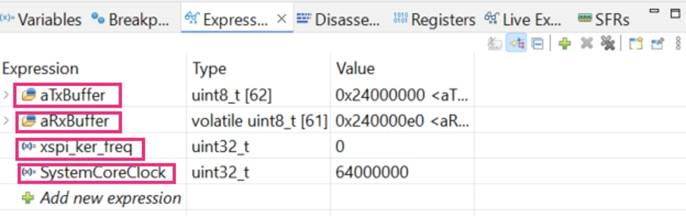
Note: The SystemCoreClock is defined in the system_stm32h7rsxxx.c file, as shown in the screenshot below.


- Click the [resume] button.

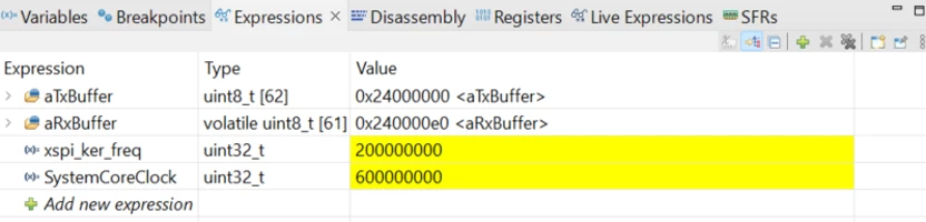
The xspi_ker_freq shows the XSPI2 kernel clock frequency, and the SystemCoreClock confirms the MCU core clock value, as shown in screenshot above.
For the aTxBuffer buffer:
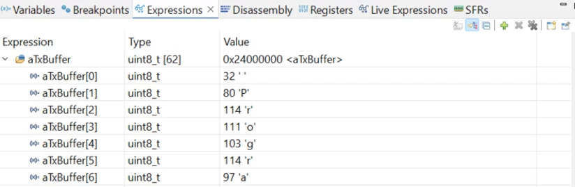
This buffer contains the data that is programmed into the external flash memory MX66UW1G45G as shown in screenshot above.
For the aRxBuffer buffer:
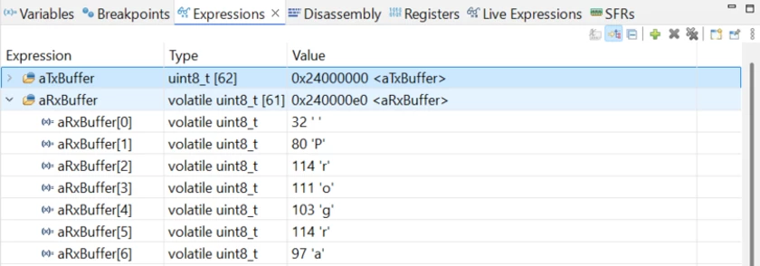
The programmed data is visible in the aRxBuffer, which stores the data read back from the external flash memory. This confirms that the content has been successfully retrieved through memory-mapped access and copied into RAM for verification as shown in the screenshot above.
In addition, the result is visible on the board: the green LED turns on, confirming that the data written to the MX66UW1G45G external flash memory was correctly read back and verified successfully, as shown in the screenshot below.
For additional verification:
- Click on [Window], click on [Show View], then select [Memory Browser], as shown in the screenshot below.
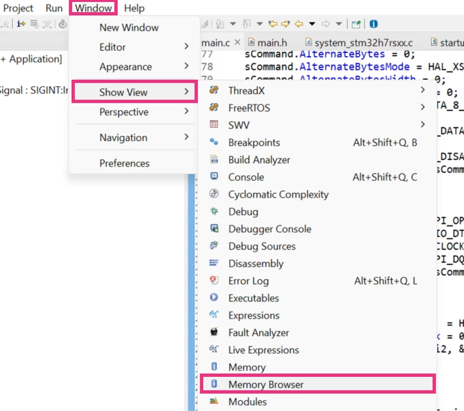
The Memory Browser is used to inspect the content of the external memory region and verify that the external memory is correctly accessible in memory-mapped mode.
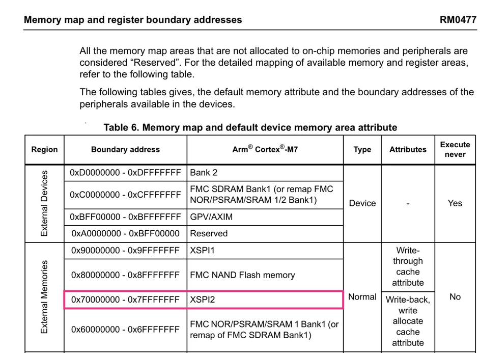
By entering the base address of the XSPI2 memory-mapped region, which is 0x70000000, the external flash can be accessed directly through its address. Once the application reaches memory-mapped mode, the programmed data appears at the XSPI2 base address location. This confirms that the write and readback sequence completed successfully, as shown in the screenshot below.

Note: The XSPI2 Base Address can be found in the Reference Manual RM0477, as shown in the screenshot below.
Conclusion
After following this guide, you are able to configure and use the external flash memory MX66UW1G45G on the STM32H7S78-DK through XSPI2.
If you want to have the final project files, you can download the extractable file attached to this article.
Related links
- Application note AN5050: Getting started with Octo-SPI, Hexadeca-SPI, and XSPI interfaces on STM32 MCUs
- User manual UM3289: Discovery kit with STM32H7S7L8 MCU
- Reference Manual RM0477: STM32H7Rx/7Sx Arm®-based 32-bit MCUs
- FAQ: Recommendations for high-speed low-voltage mode (HSLV) on the STM32H7RS
- Datasheet: STM32H7S3x8 STM32H7S7x8
- Knowledge Base Article: STM32CubeIDE: How to debug an STM32H7Rx/Sx project without flashing boot every time