Associate II
February 23, 2026
Solved

TFBGA225 Footprint on Discovery/Nucleo - why the holes, etc?

  • February 23, 2026
  • 3 replies
  • 377 views

Is there any utility in the holes and silkscreen circles around the TFBGA225 on the NUCLEO-H7S3L8?  It appears to be the same pattern on the Discovery board, suggesting it might be for BGA placement or maybe a heatsink.
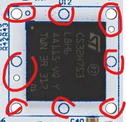
 

AndrewNeil_0-1771868357298.png


Edited to put the image in-line for better visibility

Best answer by Andrew Neil

See this thread - it's probably for a ZIF socket used internally by ST for (early?) development.

Perhaps @mƎALLEm can confirm?


PS:

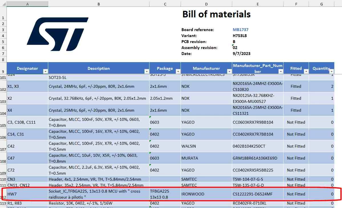
As @waclawek.jan noticed in the other thread, it's in the BoM:


Image1.jpg

3 replies

Andrew Neil
Andrew NeilBest answer
Super User
February 23, 2026

See this thread - it's probably for a ZIF socket used internally by ST for (early?) development.

Perhaps @mƎALLEm can confirm?


PS:

As @waclawek.jan noticed in the other thread, it's in the BoM:


Image1.jpg

A complex system that works is invariably found to have evolved from a simple system that worked.A complex system designed from scratch never works and cannot be patched up to make it work.
mƎALLEm
ST Technical Moderator
February 23, 2026

Hello,

These indeed are holes for a TFBGA225 socket.

The boards with socket are available only for ST internal developement usage not available on the market.

The PCB is common for the developement and market versions.


To give better visibility on the answered topics, please click "Best answer" on the reply which solved your issue or answered your question.
AlexWEI
ST Employee
May 12, 2026

Hi 

the hole and silk screen are socket for TFBGA225, if you use chips for board production, you don't need put the holes and silkscreens on .